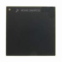
MC68EC060RC50 Freescale Semiconductor, MC68EC060RC50 Datasheet - Page 66

MC68EC060RC50
Manufacturer Part Number
MC68EC060RC50
Description
IC MPU 32BIT 50MHZ 206-PGA
Manufacturer
Freescale Semiconductor
Specifications of MC68EC060RC50
Processor Type
M680x0 32-Bit
Speed
50MHz
Voltage
3.3V
Mounting Type
Surface Mount
Package / Case
206-PGA
Family Name
M68000
Device Core
ColdFire
Device Core Size
32b
Frequency (max)
50MHz
Instruction Set Architecture
RISC
Supply Voltage 1 (typ)
3.3V
Operating Supply Voltage (max)
3.465V
Operating Supply Voltage (min)
3.135V
Operating Temp Range
0C to 110C
Operating Temperature Classification
Commercial
Mounting
Through Hole
Pin Count
206
Package Type
PGA
Lead Free Status / RoHS Status
Contains lead / RoHS non-compliant
Features
-
Lead Free Status / Rohs Status
Compliant
Available stocks
Company
Part Number
Manufacturer
Quantity
Price
Company:
Part Number:
MC68EC060RC50
Manufacturer:
NXP
Quantity:
1 746
- Current page: 66 of 416
- Download datasheet (2Mb)
Integer Unit
The operation of the instruction fetch unit (IFU) and the OEPs are decoupled by a 96-byte
FIFO instruction buffer. The IFU prefetches instructions every processor clock cycle, stop-
ping only if the instruction buffer is full or encountering a wait condition due to instruction
fetch address translation or cache miss. The OEPs attempt to read instructions from the
instruction buffer and execute them every clock cycle, stopping only if full instruction infor-
mation is not present in the buffer or due to operand pipeline wait conditions.
3.2 INTEGER UNIT REGISTER DESCRIPTION
The following paragraphs describe the integer unit registers in the user and supervisor pro-
gramming models. Refer to Section 4 Memory Management Unit for details on the MMU
programming model and Section 6 Floating-Point Unit for details on the FPU program-
ming model.
3.2.1 Integer Unit User Programming Model
Figure 3-2 illustrates the integer unit portion of the user programming model. The model is
the same as for previous M68000 family microprocessors, consisting of the following regis-
ters:
3.2.1.1 DATA REGISTERS (D7–D0). Registers D7–D0 are used as data registers for bit
and bit field (1- to 32-bit), byte (8-bit), word (16-bit), long-word (32-bit), and quad-word (64-
bit) operations. These registers may also be used as index registers.
3.2.1.2 ADDRESS REGISTERS (A6–A0). These registers can be used as software stack
pointers, index registers, or base address registers. The address registers may be used for
word and long-word operations.
3.2.1.3 USER STACK POINTER (A7). A7 is used as a hardware stack pointer during
implicit or explicit stacking for subroutine calls and exception handling. The register desig-
nation A7 refers to the user stack pointer (USP) in the user programming model and to the
3-2
• 16 General-Purpose 32-Bit Registers (D7–D0, A7–A0)
• 32-Bit Program Counter (PC)
• 8-Bit Condition Code Register (CCR)
31
31
31
Figure 3-2. Integer Unit User Programming Model
M68060 USER’S MANUAL
15
15
15
7
0
0
0
0
A0
A1
A2
A3
A4
A5
A6
A7
(USP)
PC
CCR
ADDRESS
REGISTERS
USER
STACK
POINTER
PROGRAM
COUNTER
CONDITION
CODE
REGISTER
MOTOROLA
Related parts for MC68EC060RC50
Image
Part Number
Description
Manufacturer
Datasheet
Request
R
Part Number:
Description:
Manufacturer:
Freescale Semiconductor, Inc
Datasheet:
Part Number:
Description:
Manufacturer:
Freescale Semiconductor, Inc
Datasheet:
Part Number:
Description:
Manufacturer:
Freescale Semiconductor, Inc
Datasheet:
Part Number:
Description:
Manufacturer:
Freescale Semiconductor, Inc
Datasheet:
Part Number:
Description:
Manufacturer:
Freescale Semiconductor, Inc
Datasheet:
Part Number:
Description:
Manufacturer:
Freescale Semiconductor, Inc
Datasheet:
Part Number:
Description:
Manufacturer:
Freescale Semiconductor, Inc
Datasheet:
Part Number:
Description:
Manufacturer:
Freescale Semiconductor, Inc
Datasheet:
Part Number:
Description:
Manufacturer:
Freescale Semiconductor, Inc
Datasheet:
Part Number:
Description:
Manufacturer:
Freescale Semiconductor, Inc
Datasheet:
Part Number:
Description:
Manufacturer:
Freescale Semiconductor, Inc
Datasheet:
Part Number:
Description:
Manufacturer:
Freescale Semiconductor, Inc
Datasheet:
Part Number:
Description:
Manufacturer:
Freescale Semiconductor, Inc
Datasheet:
Part Number:
Description:
Manufacturer:
Freescale Semiconductor, Inc
Datasheet:
Part Number:
Description:
Manufacturer:
Freescale Semiconductor, Inc
Datasheet:


