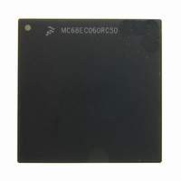
MC68EC060RC50 Freescale Semiconductor, MC68EC060RC50 Datasheet - Page 113

MC68EC060RC50
Manufacturer Part Number
MC68EC060RC50
Description
IC MPU 32BIT 50MHZ 206-PGA
Manufacturer
Freescale Semiconductor
Specifications of MC68EC060RC50
Processor Type
M680x0 32-Bit
Speed
50MHz
Voltage
3.3V
Mounting Type
Surface Mount
Package / Case
206-PGA
Family Name
M68000
Device Core
ColdFire
Device Core Size
32b
Frequency (max)
50MHz
Instruction Set Architecture
RISC
Supply Voltage 1 (typ)
3.3V
Operating Supply Voltage (max)
3.465V
Operating Supply Voltage (min)
3.135V
Operating Temp Range
0C to 110C
Operating Temperature Classification
Commercial
Mounting
Through Hole
Pin Count
206
Package Type
PGA
Lead Free Status / RoHS Status
Contains lead / RoHS non-compliant
Features
-
Lead Free Status / Rohs Status
Compliant
Available stocks
Company
Part Number
Manufacturer
Quantity
Price
Company:
Part Number:
MC68EC060RC50
Manufacturer:
NXP
Quantity:
1 746
- Current page: 113 of 416
- Download datasheet (2Mb)
Caches
5.9 STORE BUFFER
The MC68060 processor provides a four-entry store buffer (16 bytes maximum). This store
buffer is a FIFO buffer that can be used for deferring pending writes to imprecise pages to
maximize performance.
For operand writes destined for the store buffer, the operand execution pipeline incurs no
stalls. The store buffer effectively provides a measure of decoupling between the pipeline’s
ability to generate writes (one write per cycle maximum) and the ability of the system bus to
retire those writes (one write per two cycles minimum). When writing to imprecise pages,
only in the event the store buffer becomes full and there is a write operation in the EX cycle
of the operand execution pipeline will a stall be incurred.
If the store buffer is not utilized (store buffer disabled or cache inhibited, precise mode), sys-
tem bus cycles are generated directly for each pipeline write operation. The instruction is
held in the EX cycle of the operand execution pipeline (OEP) until bus transfer termination
is received. This means each write operation is stalled for a minimum of five cycles in the
EX cycle when the store buffer is not utilized.
A store buffer enable bit is contained in the CACR. This bit can be set and cleared via the
MOVEC instruction. Upon reset, this bit is cleared and all writes are precise. When the bit is
set, the cache mode generated by the MMU is used. The store buffer is utilized by the cach-
able/writethrough and the cache-inhibited/imprecise modes.
The store buffer can queue data up to four bytes in width per entry. Each entry matches a
corresponding bus cycle it will generate; therefore, a misaligned long-word write to a
writethrough page will create two entries if the address is to an odd word boundary, three
entries if to an odd byte boundary—one per bus cycle.
A misaligned write access which straddles a precise/imprecise page boundary will use the
store buffer for the imprecise portion of the write.
5.10 PUSH BUFFER AND STORE BUFFER BUS OPERATION
Once either the store buffer or the push buffer has valid data, the MC68060 bus controller
uses the next available bus cycle to generate the appropriate write cycles. In the event that
during the continued instruction execution by the processor pipeline another system bus
cycle is required (e.g., data cache miss to process, address translation cache (ATC)
tablesearch to perform), the pipeline will stall until both push and store buffers are empty
before generating the required system bus transaction.
Certain instructions and exception processing which synchronize the MC68060 processor
pipeline guarantee both push and store buffers are empty before proceeding.
5.11 BRANCH CACHE
The branch cache plays a major role in achieving the performance levels of the MC68060
processor. The branch cache provides a table associating branch program counter values
with the corresponding branch target virtual addresses. The fundamental concept is to pro-
5-14
M68060 USER’S MANUAL
MOTOROLA
Related parts for MC68EC060RC50
Image
Part Number
Description
Manufacturer
Datasheet
Request
R
Part Number:
Description:
Manufacturer:
Freescale Semiconductor, Inc
Datasheet:
Part Number:
Description:
Manufacturer:
Freescale Semiconductor, Inc
Datasheet:
Part Number:
Description:
Manufacturer:
Freescale Semiconductor, Inc
Datasheet:
Part Number:
Description:
Manufacturer:
Freescale Semiconductor, Inc
Datasheet:
Part Number:
Description:
Manufacturer:
Freescale Semiconductor, Inc
Datasheet:
Part Number:
Description:
Manufacturer:
Freescale Semiconductor, Inc
Datasheet:
Part Number:
Description:
Manufacturer:
Freescale Semiconductor, Inc
Datasheet:
Part Number:
Description:
Manufacturer:
Freescale Semiconductor, Inc
Datasheet:
Part Number:
Description:
Manufacturer:
Freescale Semiconductor, Inc
Datasheet:
Part Number:
Description:
Manufacturer:
Freescale Semiconductor, Inc
Datasheet:
Part Number:
Description:
Manufacturer:
Freescale Semiconductor, Inc
Datasheet:
Part Number:
Description:
Manufacturer:
Freescale Semiconductor, Inc
Datasheet:
Part Number:
Description:
Manufacturer:
Freescale Semiconductor, Inc
Datasheet:
Part Number:
Description:
Manufacturer:
Freescale Semiconductor, Inc
Datasheet:
Part Number:
Description:
Manufacturer:
Freescale Semiconductor, Inc
Datasheet:


