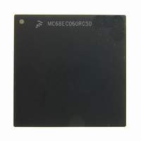
MC68EC060RC50 Freescale Semiconductor, MC68EC060RC50 Datasheet - Page 334

MC68EC060RC50
Manufacturer Part Number
MC68EC060RC50
Description
IC MPU 32BIT 50MHZ 206-PGA
Manufacturer
Freescale Semiconductor
Specifications of MC68EC060RC50
Processor Type
M680x0 32-Bit
Speed
50MHz
Voltage
3.3V
Mounting Type
Surface Mount
Package / Case
206-PGA
Family Name
M68000
Device Core
ColdFire
Device Core Size
32b
Frequency (max)
50MHz
Instruction Set Architecture
RISC
Supply Voltage 1 (typ)
3.3V
Operating Supply Voltage (max)
3.465V
Operating Supply Voltage (min)
3.135V
Operating Temp Range
0C to 110C
Operating Temperature Classification
Commercial
Mounting
Through Hole
Pin Count
206
Package Type
PGA
Lead Free Status / RoHS Status
Contains lead / RoHS non-compliant
Features
-
Lead Free Status / Rohs Status
Compliant
Available stocks
Company
Part Number
Manufacturer
Quantity
Price
Company:
Part Number:
MC68EC060RC50
Manufacturer:
NXP
Quantity:
1 746
- Current page: 334 of 416
- Download datasheet (2Mb)
Applications Information
A possible solution addressing both the address and write data hold time issue for slow
peripherals is to force at least one dead state between TA negation and TS assertion of the
next bus cycle. This can be achieved by arbitrating the bus away from the processor on any
long-word, word, or byte access. This forces the processor to release the bus, not begin a
new bus cycle, three-state the address bus, and three-state the data bus on write cycles.
Since the address and data buses (on writes) are three-stated and not directly driven by the
MC68060, output hold time in this solution relies on the capacitive loading of the bus to
achieve the extended hold time.
Once the dead state has been added, the bus is returned to the processor and normal oper-
ation continues. This suggested solution does not affect line (burst) accesses, which are typ-
ically cacheable and contain no I/O devices. For this reason, performance is not
compromised. In this implementation, the only signal that may be affected is BG. In this solu-
tion, BG is intercepted and combined with the dead-state inserting logic. This combined sig-
nal is then fed into the MC68060’s BG. Figure 11-7 shows the effect of BG.
11-12
1/2-SPEED BUS CLOCK
1/2-SPEED BUS CLOCK
Figure 11-7. MC68060 Address Hold Time Fix
Figure 11-6. MC68060 Address Hold Time
CLKEN
A[31:0]
A31–A0
CLKEN
CSX
CLK
BG
TA
TS
CLK
CS
TA
TS
M68060 USER’S MANUAL
MOTOROLA
Related parts for MC68EC060RC50
Image
Part Number
Description
Manufacturer
Datasheet
Request
R
Part Number:
Description:
Manufacturer:
Freescale Semiconductor, Inc
Datasheet:
Part Number:
Description:
Manufacturer:
Freescale Semiconductor, Inc
Datasheet:
Part Number:
Description:
Manufacturer:
Freescale Semiconductor, Inc
Datasheet:
Part Number:
Description:
Manufacturer:
Freescale Semiconductor, Inc
Datasheet:
Part Number:
Description:
Manufacturer:
Freescale Semiconductor, Inc
Datasheet:
Part Number:
Description:
Manufacturer:
Freescale Semiconductor, Inc
Datasheet:
Part Number:
Description:
Manufacturer:
Freescale Semiconductor, Inc
Datasheet:
Part Number:
Description:
Manufacturer:
Freescale Semiconductor, Inc
Datasheet:
Part Number:
Description:
Manufacturer:
Freescale Semiconductor, Inc
Datasheet:
Part Number:
Description:
Manufacturer:
Freescale Semiconductor, Inc
Datasheet:
Part Number:
Description:
Manufacturer:
Freescale Semiconductor, Inc
Datasheet:
Part Number:
Description:
Manufacturer:
Freescale Semiconductor, Inc
Datasheet:
Part Number:
Description:
Manufacturer:
Freescale Semiconductor, Inc
Datasheet:
Part Number:
Description:
Manufacturer:
Freescale Semiconductor, Inc
Datasheet:
Part Number:
Description:
Manufacturer:
Freescale Semiconductor, Inc
Datasheet:


