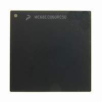
MC68EC060RC50 Freescale Semiconductor, MC68EC060RC50 Datasheet - Page 47

MC68EC060RC50
Manufacturer Part Number
MC68EC060RC50
Description
IC MPU 32BIT 50MHZ 206-PGA
Manufacturer
Freescale Semiconductor
Specifications of MC68EC060RC50
Processor Type
M680x0 32-Bit
Speed
50MHz
Voltage
3.3V
Mounting Type
Surface Mount
Package / Case
206-PGA
Family Name
M68000
Device Core
ColdFire
Device Core Size
32b
Frequency (max)
50MHz
Instruction Set Architecture
RISC
Supply Voltage 1 (typ)
3.3V
Operating Supply Voltage (max)
3.465V
Operating Supply Voltage (min)
3.135V
Operating Temp Range
0C to 110C
Operating Temperature Classification
Commercial
Mounting
Through Hole
Pin Count
206
Package Type
PGA
Lead Free Status / RoHS Status
Contains lead / RoHS non-compliant
Features
-
Lead Free Status / Rohs Status
Compliant
Available stocks
Company
Part Number
Manufacturer
Quantity
Price
Company:
Part Number:
MC68EC060RC50
Manufacturer:
NXP
Quantity:
1 746
- Current page: 47 of 416
- Download datasheet (2Mb)
SECTION 2
SIGNAL DESCRIPTION
This section contains brief descriptions of the MC68060 signals in their functional groups
(see Figure 2-1). Each signal’s function is briefly explained, referencing other sections con-
taining detailed information about the signal and related operations. Table 2-1 lists the
MC68060 signal names, mnemonics, and functional descriptions of the signals. Timing
specifications for these signals can be found in Section 12 Electrical and Thermal Char-
acteristics .
MOTOROLA
Address Bus
Cycle Long-Word Ad-
dress
Data Bus
Transfer Type
Transfer Modifier
Transfer Line Number
User-Programmable
Attributes
Read/Write
Transfer Size
Bus Lock
Bus Lock End
Cache Inhibit Out
Byte Select
Transfer Start
Transfer in Progress
Starting Termination Ac-
knowledge Signal Sam-
pling
Transfer Acknowledge
Signal Name
Assertion and negation are used to specify forcing a signal to a
particular state. Assertion and assert refer to a signal that is ac-
tive or true. Negation and negate refer to a signal that is inactive
or false. These terms are used independently of the voltage level
(high or low) that they represent.
UPA1,UPA0 User-defined signals, controlled by the corresponding user attribute bits from the
TLN1,TLN0 Indicates which cache line in a set is being pushed or loaded by the current line
Mnemonic
TM2–TM0
SIZ1,SIZ0
BS3–BS0
TT1,TT0
D31–D0
A31–A0
LOCKE
CIOUT
LOCK
CLA
R/W
SAS
TIP
TS
TA
Controls the operation of A3 and A2 during bus cycles.
Indicates the general transfer type: normal, MOVE16, alternate logical function
code, and acknowledge.
transfer cycle.
address translation entry.
Identifies the transfer as a read or write.
Indicates the data transfer size. These signals, together with A0 and A1,
define the active sections of the data bus. Alternately, BS3–BS0 can be used for
this function.
Indicates a bus cycle is part of a read-modify-write operation and that the
sequence of bus cycles should not be interrupted.
Indicates the current bus cycle is the last in a locked sequence of bus cycles.
Indicates the processor will not cache the current bus transfer information.
Indicate which bytes within a long word are selected and which data bus bytes
are valid.
Indicates the beginning of a bus cycle.
Asserted for the duration of a bus cycle.
Indicates the MC68060 will begin sampling the termination acknowledge signals.
Asserted to acknowledge a bus transfer.
32-bit address bus used to address any of 4-Gbytes.
32-bit data bus used to transfer up to 32 bits of data per bus transfer.
Indicates supplemental information about the access.
Table 2-1. Signal Index
M68060 USER’S MANUAL
NOTE
Function
2-1
Related parts for MC68EC060RC50
Image
Part Number
Description
Manufacturer
Datasheet
Request
R
Part Number:
Description:
Manufacturer:
Freescale Semiconductor, Inc
Datasheet:
Part Number:
Description:
Manufacturer:
Freescale Semiconductor, Inc
Datasheet:
Part Number:
Description:
Manufacturer:
Freescale Semiconductor, Inc
Datasheet:
Part Number:
Description:
Manufacturer:
Freescale Semiconductor, Inc
Datasheet:
Part Number:
Description:
Manufacturer:
Freescale Semiconductor, Inc
Datasheet:
Part Number:
Description:
Manufacturer:
Freescale Semiconductor, Inc
Datasheet:
Part Number:
Description:
Manufacturer:
Freescale Semiconductor, Inc
Datasheet:
Part Number:
Description:
Manufacturer:
Freescale Semiconductor, Inc
Datasheet:
Part Number:
Description:
Manufacturer:
Freescale Semiconductor, Inc
Datasheet:
Part Number:
Description:
Manufacturer:
Freescale Semiconductor, Inc
Datasheet:
Part Number:
Description:
Manufacturer:
Freescale Semiconductor, Inc
Datasheet:
Part Number:
Description:
Manufacturer:
Freescale Semiconductor, Inc
Datasheet:
Part Number:
Description:
Manufacturer:
Freescale Semiconductor, Inc
Datasheet:
Part Number:
Description:
Manufacturer:
Freescale Semiconductor, Inc
Datasheet:
Part Number:
Description:
Manufacturer:
Freescale Semiconductor, Inc
Datasheet:


