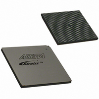
EP1S40B956C5 Altera, EP1S40B956C5 Datasheet - Page 712

EP1S40B956C5
Manufacturer Part Number
EP1S40B956C5
Description
IC STRATIX FPGA 40K LE 956-BGA
Manufacturer
Altera
Series
Stratix®r
Datasheet
1.EP1S10F484I6N.pdf
(864 pages)
Specifications of EP1S40B956C5
Number Of Logic Elements/cells
41250
Number Of Labs/clbs
4125
Total Ram Bits
3423744
Number Of I /o
683
Voltage - Supply
1.425 V ~ 1.575 V
Mounting Type
Surface Mount
Operating Temperature
0°C ~ 85°C
Package / Case
956-BGA
Lead Free Status / RoHS Status
Contains lead / RoHS non-compliant
Number Of Gates
-
Available stocks
Company
Part Number
Manufacturer
Quantity
Price
Part Number:
EP1S40B956C5
Manufacturer:
ALTERA/阿尔特拉
Quantity:
20 000
- Current page: 712 of 864
- Download datasheet (11Mb)
I/O Structure
10–28
Stratix Device Handbook, Volume 2
The differential I/O within Stratix GX also provides dynamic phase
alignment (DPA). DPA enables the differential I/O to operate up to
1 Gbps per channel. DPA automatically and continuously tracks
fluctuations caused by system variations and self-adjusts to eliminate the
phase skew between the multiplied clock and the serial data. The block
contains a dynamic phase selector for phase detection and selection, a
SERDES, a synchronizer, and a data realigner circuit. You can bypass the
dynamic phase aligner without affecting the basic source-synchronous
operation of the channel by using a separate deserializer.
If you compile an APEX II LVDS design that uses clock-data
synchronization (CDS) for a Stratix or Stratix GX device, the Quartus II
software issues a warning during compilation that Stratix and Stratix GX
devices do not support CDS.
Stratix and Stratix GX devices offer a flexible solution using new byte
realignment circuitry to correct for byte misalignment by shifting, or
slipping, data bits. Stratix and Stratix GX devices activate the byte
realignment circuitry when an external pin (rx_data_align) or an
internal custom-made state machine asserts the SYNC node high.
APEX II, APEX 20KE, and APEX 20KCdevices have a dedicated
transmitter clock output pin (LVDSTXOUTCLK). In Stratix and Stratix GX
devices, a transmitter dataout channel with an LVDS clock (fast clock)
generates the transmitter clock output. Therefore, you can drive any
Note to
(1)
EP1SGX10 C
EP1SGX10 D
EP1SGX25 C
EP1SGX25 D
EP1SGX25 F
EP1SGX40 D
EP1SGX40 G
Table 10–10. Number of Dedicated DIfferential Channels in Stratix GX
Devices
Device
For information on channel speeds, see the Stratix GX Device Family Data Sheet
section of the Stratix GX Device Handbook, Volume 1 and the High-Speed
Source-Synchronous Differential I/O Interfaces in Stratix GX Devices chapter of the
Stratix GX Device Handbook, Volume 2.
Table
Note (1)
10–10:
672/1,020
Pin Count
1,020
1,020
1,020
672
672
672
Transceivers
Number of
16
20
4
8
4
8
8
Number of Source-
Altera Corporation
Synchronous
Channels
22
22
39
39
39
45
45
July 2005
Related parts for EP1S40B956C5
Image
Part Number
Description
Manufacturer
Datasheet
Request
R

Part Number:
Description:
CYCLONE II STARTER KIT EP2C20N
Manufacturer:
Altera
Datasheet:

Part Number:
Description:
CPLD, EP610 Family, ECMOS Process, 300 Gates, 16 Macro Cells, 16 Reg., 16 User I/Os, 5V Supply, 35 Speed Grade, 24DIP
Manufacturer:
Altera Corporation
Datasheet:

Part Number:
Description:
CPLD, EP610 Family, ECMOS Process, 300 Gates, 16 Macro Cells, 16 Reg., 16 User I/Os, 5V Supply, 15 Speed Grade, 24DIP
Manufacturer:
Altera Corporation
Datasheet:

Part Number:
Description:
Manufacturer:
Altera Corporation
Datasheet:

Part Number:
Description:
CPLD, EP610 Family, ECMOS Process, 300 Gates, 16 Macro Cells, 16 Reg., 16 User I/Os, 5V Supply, 30 Speed Grade, 24DIP
Manufacturer:
Altera Corporation
Datasheet:

Part Number:
Description:
High-performance, low-power erasable programmable logic devices with 8 macrocells, 10ns
Manufacturer:
Altera Corporation
Datasheet:

Part Number:
Description:
High-performance, low-power erasable programmable logic devices with 8 macrocells, 7ns
Manufacturer:
Altera Corporation
Datasheet:

Part Number:
Description:
Classic EPLD
Manufacturer:
Altera Corporation
Datasheet:

Part Number:
Description:
High-performance, low-power erasable programmable logic devices with 8 macrocells, 10ns
Manufacturer:
Altera Corporation
Datasheet:

Part Number:
Description:
Manufacturer:
Altera Corporation
Datasheet:

Part Number:
Description:
Manufacturer:
Altera Corporation
Datasheet:

Part Number:
Description:
Manufacturer:
Altera Corporation
Datasheet:

Part Number:
Description:
CPLD, EP610 Family, ECMOS Process, 300 Gates, 16 Macro Cells, 16 Reg., 16 User I/Os, 5V Supply, 25 Speed Grade, 24DIP
Manufacturer:
Altera Corporation
Datasheet:


