EP1S40B956C5 Altera, EP1S40B956C5 Datasheet - Page 467
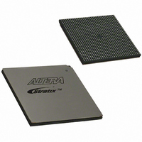
EP1S40B956C5
Manufacturer Part Number
EP1S40B956C5
Description
IC STRATIX FPGA 40K LE 956-BGA
Manufacturer
Altera
Series
Stratix®r
Datasheet
1.EP1S10F484I6N.pdf
(864 pages)
Specifications of EP1S40B956C5
Number Of Logic Elements/cells
41250
Number Of Labs/clbs
4125
Total Ram Bits
3423744
Number Of I /o
683
Voltage - Supply
1.425 V ~ 1.575 V
Mounting Type
Surface Mount
Operating Temperature
0°C ~ 85°C
Package / Case
956-BGA
Lead Free Status / RoHS Status
Contains lead / RoHS non-compliant
Number Of Gates
-
Available stocks
Company
Part Number
Manufacturer
Quantity
Price

Part Number:
EP1S40B956C5
Manufacturer:
ALTERA/阿尔特拉
Quantity:
20 000


Altera Corporation
June 2006
Device & Pin Options
Click Device & Pin Options in the Compiler Settings dialog box to
access the I/O pin settings. For example, in the Voltage tab you can select
a default I/O standard for all pins for the targeted device. I/O pins that
do not have a specific I/O standard assignment default this standard.
Click OK when you are done setting I/O pin options to return to the
Compiler Settings dialog box.
Assign Pins
Click Assign Pins in the Compiler Settings dialog box to view the
device’s pin settings and pin assignments (see
the pin settings under Available Pins & Existing Assignments. The
listing does not include V
information for each pin includes:
■
■
■
■
■
■
■
■
Figure 4–23. Assign Pins
Number
Name
I/O Bank
I/O Standard
Type (e.g., row or column I/O and differential or control)
SignalProbe Source Name
Enabled (that is, whether SignalProbe routing is enabled or disabled
Status
Selectable I/O Standards in Stratix & Stratix GX Devices
REF
pins because they are dedicated pins. The
Stratix Device Handbook, Volume 2
Figure
4–23). You can view
4–39
Related parts for EP1S40B956C5
Image
Part Number
Description
Manufacturer
Datasheet
Request
R

Part Number:
Description:
CYCLONE II STARTER KIT EP2C20N
Manufacturer:
Altera
Datasheet:


Part Number:
Description:
CPLD, EP610 Family, ECMOS Process, 300 Gates, 16 Macro Cells, 16 Reg., 16 User I/Os, 5V Supply, 35 Speed Grade, 24DIP
Manufacturer:
Altera Corporation
Datasheet:
Part Number:
Description:
CPLD, EP610 Family, ECMOS Process, 300 Gates, 16 Macro Cells, 16 Reg., 16 User I/Os, 5V Supply, 15 Speed Grade, 24DIP
Manufacturer:
Altera Corporation
Datasheet:
Part Number:
Description:
Manufacturer:
Altera Corporation
Datasheet:
Part Number:
Description:
CPLD, EP610 Family, ECMOS Process, 300 Gates, 16 Macro Cells, 16 Reg., 16 User I/Os, 5V Supply, 30 Speed Grade, 24DIP
Manufacturer:
Altera Corporation
Datasheet:
Part Number:
Description:
High-performance, low-power erasable programmable logic devices with 8 macrocells, 10ns
Manufacturer:
Altera Corporation
Datasheet:
Part Number:
Description:
High-performance, low-power erasable programmable logic devices with 8 macrocells, 7ns
Manufacturer:
Altera Corporation
Datasheet:
Part Number:
Description:
Classic EPLD
Manufacturer:
Altera Corporation
Datasheet:
Part Number:
Description:
High-performance, low-power erasable programmable logic devices with 8 macrocells, 10ns
Manufacturer:
Altera Corporation
Datasheet:
Part Number:
Description:
Manufacturer:
Altera Corporation
Datasheet:
Part Number:
Description:
Manufacturer:
Altera Corporation
Datasheet:
Part Number:
Description:
Manufacturer:
Altera Corporation
Datasheet:
Part Number:
Description:
CPLD, EP610 Family, ECMOS Process, 300 Gates, 16 Macro Cells, 16 Reg., 16 User I/Os, 5V Supply, 25 Speed Grade, 24DIP
Manufacturer:
Altera Corporation
Datasheet: