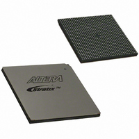
EP1S40B956C5 Altera, EP1S40B956C5 Datasheet - Page 402

EP1S40B956C5
Manufacturer Part Number
EP1S40B956C5
Description
IC STRATIX FPGA 40K LE 956-BGA
Manufacturer
Altera
Series
Stratix®r
Datasheet
1.EP1S10F484I6N.pdf
(864 pages)
Specifications of EP1S40B956C5
Number Of Logic Elements/cells
41250
Number Of Labs/clbs
4125
Total Ram Bits
3423744
Number Of I /o
683
Voltage - Supply
1.425 V ~ 1.575 V
Mounting Type
Surface Mount
Operating Temperature
0°C ~ 85°C
Package / Case
956-BGA
Lead Free Status / RoHS Status
Contains lead / RoHS non-compliant
Number Of Gates
-
Available stocks
Company
Part Number
Manufacturer
Quantity
Price
Part Number:
EP1S40B956C5
Manufacturer:
ALTERA/阿尔特拉
Quantity:
20 000
- Current page: 402 of 864
- Download datasheet (11Mb)
External Memory Standards
Figure 3–4. QDR SRAM Block Diagram for Burst-of-Two Architecture
3–6
Stratix Device Handbook, Volume 2
WPSn
BWSn
K, Kn
V
REF
D
A
18
18
Discrete QDR SRAM Device
2
same scheme as in DDR SDRAM interfaces whereby the dedicated
circuitry is used during reads to center-align the data and the read clock
inside the FPGA and the PLL center-aligns the data and write clock
outputs. The data and clock relationship for reads and writes in
RLDRAM II is similar to those in DDR SDRAM as already depicted in
Figure 3–1 on page 3–3
QDR & QDRII SRAM
QDR SRAM provides independent read and write ports that eliminate
the need for bus turnaround. The memory uses two sets of clocks: K and
Kn for write access, and optional C and Cn for read accesses, where Kn
and Cn are the inverse of the K and C clocks, respectively. You can use
differential HSTL I/O pins to drive the QDR SRAM clock into the Stratix
and Stratix GX devices. The separate write data and read data ports
permit a transfer rate up to four words on every cycle through the DDR
circuitry. Stratix and Stratix GX devices support both burst-of-two and
burst-of-four QDR SRAM architectures, with clock cycles up to 167 MHz
using the 1.5-V HSTL Class I or Class II I/O standard.
the block diagram for QDR SRAM burst-of-two architecture.
QDRII SRAM is a second generation of QDR SRAM devices. It can
transfer four words per clock cycle, fulfilling the requirements facing
next-generation communications system designers. QDRII SRAM
devices provide concurrent reads and writes, zero latency, and increased
data throughput. Stratix and Stratix GX devices support QDRII SRAM at
speeds up to 200 MHz since the timing requirements for QDRII SRAM
are not as strict as QDR SRAM.
Write
Port
Control
Logic
36
Data
256K × 18
Memory
Array
256K × 18
and
Memory
Array
Figure 3–3 on page
36
Data
Read
Port
3–4.
18
2
Figure 3–4
Altera Corporation
RPSn
C, Cn
Q
June 2006
shows
Related parts for EP1S40B956C5
Image
Part Number
Description
Manufacturer
Datasheet
Request
R

Part Number:
Description:
CYCLONE II STARTER KIT EP2C20N
Manufacturer:
Altera
Datasheet:

Part Number:
Description:
CPLD, EP610 Family, ECMOS Process, 300 Gates, 16 Macro Cells, 16 Reg., 16 User I/Os, 5V Supply, 35 Speed Grade, 24DIP
Manufacturer:
Altera Corporation
Datasheet:

Part Number:
Description:
CPLD, EP610 Family, ECMOS Process, 300 Gates, 16 Macro Cells, 16 Reg., 16 User I/Os, 5V Supply, 15 Speed Grade, 24DIP
Manufacturer:
Altera Corporation
Datasheet:

Part Number:
Description:
Manufacturer:
Altera Corporation
Datasheet:

Part Number:
Description:
CPLD, EP610 Family, ECMOS Process, 300 Gates, 16 Macro Cells, 16 Reg., 16 User I/Os, 5V Supply, 30 Speed Grade, 24DIP
Manufacturer:
Altera Corporation
Datasheet:

Part Number:
Description:
High-performance, low-power erasable programmable logic devices with 8 macrocells, 10ns
Manufacturer:
Altera Corporation
Datasheet:

Part Number:
Description:
High-performance, low-power erasable programmable logic devices with 8 macrocells, 7ns
Manufacturer:
Altera Corporation
Datasheet:

Part Number:
Description:
Classic EPLD
Manufacturer:
Altera Corporation
Datasheet:

Part Number:
Description:
High-performance, low-power erasable programmable logic devices with 8 macrocells, 10ns
Manufacturer:
Altera Corporation
Datasheet:

Part Number:
Description:
Manufacturer:
Altera Corporation
Datasheet:

Part Number:
Description:
Manufacturer:
Altera Corporation
Datasheet:

Part Number:
Description:
Manufacturer:
Altera Corporation
Datasheet:

Part Number:
Description:
CPLD, EP610 Family, ECMOS Process, 300 Gates, 16 Macro Cells, 16 Reg., 16 User I/Os, 5V Supply, 25 Speed Grade, 24DIP
Manufacturer:
Altera Corporation
Datasheet:


