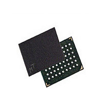
MT48H8M16LFB4-75 IT:J Micron Technology Inc, MT48H8M16LFB4-75 IT:J Datasheet - Page 72

MT48H8M16LFB4-75 IT:J
Manufacturer Part Number
MT48H8M16LFB4-75 IT:J
Description
Manufacturer
Micron Technology Inc
Type
Mobile SDRAMr
Datasheet
1.MT48H8M16LFB4-75_ITJ.pdf
(75 pages)
Specifications of MT48H8M16LFB4-75 IT:J
Organization
8Mx16
Density
128Mb
Address Bus
14b
Access Time (max)
8/5.4ns
Maximum Clock Rate
133MHz
Operating Supply Voltage (typ)
1.8V
Package Type
VFBGA
Operating Temp Range
-40C to 85C
Operating Supply Voltage (max)
1.95V
Operating Supply Voltage (min)
1.7V
Supply Current
70mA
Pin Count
54
Mounting
Surface Mount
Operating Temperature Classification
Industrial
Lead Free Status / Rohs Status
Compliant
Deep Power-Down
Clock Suspend
Figure 51:
PDF: 09005aef832ff1ea/Source: 09005aef832ff1ac
sdr_mobile_sdram_cmd_op_timing_dia_fr10_08__3.fm - Rev. E 4/09 EN
Clock Suspend During WRITE Burst
Notes:
Deep power-down mode is a maximum power-saving feature achieved by shutting off
the power to the entire device memory array. Data on the memory array will not be
retained after deep power-down mode is executed. Deep power-down mode is entered
by having all banks idle, with CS# and WE# held LOW with RAS# and CAS# HIGH at the
rising edge of the clock, while CKE is LOW. CKE must be held LOW during deep power-
down.
To exit deep power-down mode, CKE must be asserted HIGH. Upon exiting deep power-
down mode, a full initialization sequence is required.
The clock suspend mode occurs when a column access/burst is in progress and CKE is
registered LOW. In the clock suspend mode, the internal clock is deactivated, “freezing”
the synchronous logic.
For each positive clock edge on which CKE is sampled LOW, the next internal positive
clock edge is suspended. Any command or data present on the input balls when an
internal clock edge is suspended will be ignored; any data present on the DQ balls
remains driven; and burst counters are not incremented, as long as the clock is
suspended (see examples in Figure 51, and Figure 52 on page 73).
Exit clock suspend mode by registering CKE HIGH; the internal clock and related opera-
tion will resume on the subsequent positive clock edge.
1. For this example, BL = 4 or greater, and DQM is LOW.
Command
Internal
Address
clock
CKE
CLK
Din
NOP
T0
WRITE
Bank,
Col n
Din
T1
n
128Mb: 8 Meg x 16, 4 Meg x 32 Mobile SDRAM
72
T2
Micron Technology, Inc., reserves the right to change products or specifications without notice.
T3
NOP
n + 1
Din
T4
Don’t Care
NOP
n + 2
T5
Din
©2008 Micron Technology, Inc. All rights reserved.
Timing Diagrams


