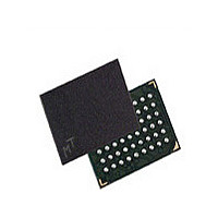
MT48H8M16LFB4-75 IT:J Micron Technology Inc, MT48H8M16LFB4-75 IT:J Datasheet - Page 34

MT48H8M16LFB4-75 IT:J
Manufacturer Part Number
MT48H8M16LFB4-75 IT:J
Description
Manufacturer
Micron Technology Inc
Type
Mobile SDRAMr
Datasheet
1.MT48H8M16LFB4-75_ITJ.pdf
(75 pages)
Specifications of MT48H8M16LFB4-75 IT:J
Organization
8Mx16
Density
128Mb
Address Bus
14b
Access Time (max)
8/5.4ns
Maximum Clock Rate
133MHz
Operating Supply Voltage (typ)
1.8V
Package Type
VFBGA
Operating Temp Range
-40C to 85C
Operating Supply Voltage (max)
1.95V
Operating Supply Voltage (min)
1.7V
Supply Current
70mA
Pin Count
54
Mounting
Surface Mount
Operating Temperature Classification
Industrial
Lead Free Status / Rohs Status
Compliant
Table 18:
Initialization
PDF: 09005aef832ff1ea/Source: 09005aef832ff1ac
sdr_mobile_sdram_cmd_op_timing_dia_fr10_08__3.fm - Rev. E 4/09 EN
CKE
H
H
L
L
n-1
Truth Table – CKE
Notes 1–4 apply to all parameters in this table; notes appear below table
CKE
H
H
L
L
n
Notes:
Reading or writing
Deep power-down
Deep power-down
Current State
Clock suspend
Clock suspend
All banks idle
All banks idle
All banks idle
Power-down
Power-down
Self refresh
Self refresh
1. CKE
2. Current state is the state of the SDRAM immediately prior to clock edge n.
3. COMMAND
4. All states and sequences not shown are illegal or reserved.
5. Exiting power-down at clock edge n will put the device in the all-banks-idle state in time for
6. Exiting self refresh at clock edge n will put the device in the all-banks-idle state after
7. After exiting clock suspend at clock edge n, the device will resume operation and recognize
8. Deep power-down is a power-saving feature of this Mobile SDRAM device. This command is
Low-power SDRAM devices must be powered up and initialized in a predefined manner.
Using initialization procedures other than those specified may result in undefined oper-
ation. After power is simultaneously applied to V
(stable clock is defined as a signal cycling within timing constraints specified for the
clock ball), the SDRAM requires a 100µs delay prior to issuing any command other than
a COMMAND INHIBIT or NOP. Starting at some point during this 100µs period and
continuing at least through the end of this period, COMMAND INHIBIT or NOP
commands should be applied.
After the 100µs delay is satisfied by issuing at least one COMMAND INHIBIT or NOP
command, a PRECHARGE command must be issued. All banks must then be
precharged, which places the device in the all-banks-idle state.
clock edge.
of COMMAND
clock edge n + 1 (provided that
met. COMMAND INHIBIT or NOP commands should be issued on any clock edges occurring
during the
t
the next command at clock edge n + 1.
BURST TERMINATE when CKE is HIGH and DEEP POWER-DOWN when CKE is LOW.
XSR period.
n
is the logic state of CKE at clock edge n; CKE
t
n
XSR period. A minimum of two NOP commands must be provided during the
is the command registered at clock edge n, and ACTION
n
.
COMMAND INHIBIT or NOP
COMMAND INHIBIT or NOP
COMMAND INHIBIT or NOP
Table 17 on page 32
BURST TERMINATE
AUTO REFRESH
128Mb: 8 Meg x 16, 4 Meg x 32 Mobile SDRAM
Command
34
VALID
X
X
X
X
X
X
t
CKS is met).
n
Micron Technology, Inc., reserves the right to change products or specifications without notice.
DD
n-1
and V
Maintain deep power-down
was the state of CKE at the previous
Deep power-down entry
Maintain clock suspend
Exit deep power-down
Maintain power-down
Maintain self refresh
Clock suspend entry
Power-down entry
Exit clock suspend
Self refresh entry
Exit power-down
DD
Exit self refresh
Q and the clock is stable
Action
©2008 Micron Technology, Inc. All rights reserved.
n
n
is a result
Initialization
Notes
t
XSR is
5
6
7
8


