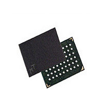
MT48H8M16LFB4-75 IT:J Micron Technology Inc, MT48H8M16LFB4-75 IT:J Datasheet - Page 54

MT48H8M16LFB4-75 IT:J
Manufacturer Part Number
MT48H8M16LFB4-75 IT:J
Description
Manufacturer
Micron Technology Inc
Type
Mobile SDRAMr
Datasheet
1.MT48H8M16LFB4-75_ITJ.pdf
(75 pages)
Specifications of MT48H8M16LFB4-75 IT:J
Organization
8Mx16
Density
128Mb
Address Bus
14b
Access Time (max)
8/5.4ns
Maximum Clock Rate
133MHz
Operating Supply Voltage (typ)
1.8V
Package Type
VFBGA
Operating Temp Range
-40C to 85C
Operating Supply Voltage (max)
1.95V
Operating Supply Voltage (min)
1.7V
Supply Current
70mA
Pin Count
54
Mounting
Surface Mount
Operating Temperature Classification
Industrial
Lead Free Status / Rohs Status
Compliant
Figure 31:
PDF: 09005aef832ff1ea/Source: 09005aef832ff1ac
sdr_mobile_sdram_cmd_op_timing_dia_fr10_08__3.fm - Rev. E 4/09 EN
WRITE-to-PRECHARGE
Notes:
1. In this example DQM could remain LOW if the WRITE burst is a fixed length of two.
Fixed-length WRITE bursts can be truncated with the BURST TERMINATE command.
When truncating a WRITE burst, the input data applied coincident with the BURST
TERMINATE command is ignored. The last data written (provided that DQM is LOW at
that time) will be the input data applied one clock previous to the BURST TERMINATE
command. This is shown in Figure 32 on page 55, where data n is the last desired data
element of a longer burst.
t
t
Command
Command
WR @
WR @
Address
Address
DQM
DQM
CLK
t
t
DQ
DQ
CK
CK < 15ns
15ns
WRITE
Bank a,
WRITE
Bank a,
Col n
Din
Col n
Din
T0
n
n
n + 1
n + 1
NOP
NOP
Din
Din
T1
128Mb: 8 Meg x 16, 4 Meg x 32 Mobile SDRAM
t
WR
54
PRECHARGE
(a or all)
Bank
NOP
T2
t
WR
Micron Technology, Inc., reserves the right to change products or specifications without notice.
PRECHARGE
(a or all)
Bank
T3
NOP
t RP
NOP
NOP
T4
t RP
ACTIVE
Bank a,
NOP
Row
T5
©2008 Micron Technology, Inc. All rights reserved.
Timing Diagrams
Don’t Care
ACTIVE
Bank a,
NOP
Row
T6


