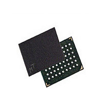
MT48H8M16LFB4-75 IT:J Micron Technology Inc, MT48H8M16LFB4-75 IT:J Datasheet - Page 27

MT48H8M16LFB4-75 IT:J
Manufacturer Part Number
MT48H8M16LFB4-75 IT:J
Description
Manufacturer
Micron Technology Inc
Type
Mobile SDRAMr
Datasheet
1.MT48H8M16LFB4-75_ITJ.pdf
(75 pages)
Specifications of MT48H8M16LFB4-75 IT:J
Organization
8Mx16
Density
128Mb
Address Bus
14b
Access Time (max)
8/5.4ns
Maximum Clock Rate
133MHz
Operating Supply Voltage (typ)
1.8V
Package Type
VFBGA
Operating Temp Range
-40C to 85C
Operating Supply Voltage (max)
1.95V
Operating Supply Voltage (min)
1.7V
Supply Current
70mA
Pin Count
54
Mounting
Surface Mount
Operating Temperature Classification
Industrial
Lead Free Status / Rohs Status
Compliant
READ
Figure 10:
WRITE
PDF: 09005aef832ff1ea/Source: 09005aef832ff1ac
sdr_mobile_sdram_cmd_op_timing_dia_fr10_08__3.fm - Rev. E 4/09 EN
READ Command
Notes:
The READ command is used to initiate a burst read access to an active row. The values
on the BA0 and BA1 inputs select the bank; the address provided selects the starting
column location. The value on input A10 determines whether auto precharge is used. If
auto precharge is selected, the row being accessed is precharged at the end of the READ
burst; if auto precharge is not selected, the row remains open for subsequent accesses.
Read data appears on the DQ subject to the logic level on the DQM inputs two clocks
earlier. If a given DQM signal was registered HIGH, the corresponding DQ will be High-Z
two clocks later; if the DQM signal was registered LOW, the DQ will provide valid data.
Figure 10 shows the READ command.
1. EN AP = enable auto precharge, DIS AP = disable auto precharge
The WRITE command is used to initiate a burst write access to an active row. The values
on the BA0 and BA1 inputs select the bank; the address provided selects the starting
column location. The value on input A10 determines whether auto precharge is used. If
auto precharge is selected, the row being accessed is precharged at the end of the write
burst; if auto precharge is not selected, the row remains open for subsequent accesses.
Input data appearing on the DQ is written to the memory array subject to the DQM
input logic level appearing coincident with the data. If a given DQM signal is registered
LOW, the corresponding data is written to memory; if the DQM signal is registered
HIGH, the corresponding data inputs are ignored and a WRITE is not executed to that
byte/column location. Figure 11 shows the WRITE command.
BA0, BA1
Address
RAS#
CAS#
A10
WE#
CKE
CLK
CS#
1
HIGH
Column address
Bank address
128Mb: 8 Meg x 16, 4 Meg x 32 Mobile SDRAM
DIS AP
EN AP
27
Don’t Care
Micron Technology, Inc., reserves the right to change products or specifications without notice.
©2008 Micron Technology, Inc. All rights reserved.
Commands


