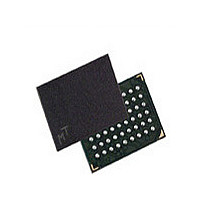
MT48H8M16LFB4-75 IT:J Micron Technology Inc, MT48H8M16LFB4-75 IT:J Datasheet - Page 41

MT48H8M16LFB4-75 IT:J
Manufacturer Part Number
MT48H8M16LFB4-75 IT:J
Description
Manufacturer
Micron Technology Inc
Type
Mobile SDRAMr
Datasheet
1.MT48H8M16LFB4-75_ITJ.pdf
(75 pages)
Specifications of MT48H8M16LFB4-75 IT:J
Organization
8Mx16
Density
128Mb
Address Bus
14b
Access Time (max)
8/5.4ns
Maximum Clock Rate
133MHz
Operating Supply Voltage (typ)
1.8V
Package Type
VFBGA
Operating Temp Range
-40C to 85C
Operating Supply Voltage (max)
1.95V
Operating Supply Voltage (min)
1.7V
Supply Current
70mA
Pin Count
54
Mounting
Surface Mount
Operating Temperature Classification
Industrial
Lead Free Status / Rohs Status
Compliant
Output Drive Strength
Bank/Row Activation
Figure 17:
PDF: 09005aef832ff1ea/Source: 09005aef832ff1ac
sdr_mobile_sdram_cmd_op_timing_dia_fr10_08__3.fm - Rev. E 4/09 EN
Example: Meeting
WRITE and READ commands can still be issued to any bank selected during standard
operation, but only the selected banks or segments of a bank in PASR are refreshed
during self refresh. It is important to note that data in unused banks or portions of banks
is lost when PASR is used.
Because the Mobile SDRAM is designed for use in smaller systems that are typically
point-to-point connections, an option to control the drive strength of the output buffers
is provided. Drive strength should be selected based on the expected loading of the
memory bus. There are four supported settings for the output drivers: 25Ω, 37Ω, 55Ω,
and 80Ω internal impedance. These are full, three-quarter, one-half, and one-quarter
drive strengths, respectively.
Before any READ or WRITE commands can be issued to a bank within the SDRAM, a row
in that bank must be “opened.” This is accomplished via the ACTIVE command, that
selects both the bank and the row to be activated (see Figure 17).
After opening a row is opened with the ACTIVE command, a READ or WRITE command
can be issued to that row, subject to the
divided by the clock period and rounded up to the next whole number to determine the
earliest clock edge after the ACTIVE command on which a READ or WRITE command
can be entered. For example, a
period) results in 2.5 clocks, rounded to 3. This is reflected in Figure 17, which covers any
case where 2 <
fication limits from time units to clock cycles.)
A subsequent ACTIVE command to a different row in the same bank can only be issued
after the previous active row has been “closed” (precharged). The minimum time
interval between successive ACTIVE commands to the same bank is defined by
A subsequent ACTIVE command to another bank can be issued while the first bank is
being accessed, which results in a reduction of total row-access overhead. The minimum
time interval between successive ACTIVE commands to different banks is defined by
t
Command
RRD.
CLK
t
RCD (MIN) When 2 <
ACTIVE
T0
t
RCD (MIN)/
t CK
NOP
t
RCD (MIN)
128Mb: 8 Meg x 16, 4 Meg x 32 Mobile SDRAM
T1
t
CK ≤ 3. (The same procedure is used to convert other speci-
41
t
RCD specification of 20ns with a 125 MHz clock (8ns
t CK
t
RCD (MIN)/
NOP
Micron Technology, Inc., reserves the right to change products or specifications without notice.
t
RCD specification.
T2
t CK
t
CK < 3
READ or
WRITE
Don’t Care
T3
t
RCD (MIN) should be
©2008 Micron Technology, Inc. All rights reserved.
Register Definition
t
RC.


