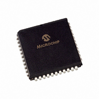
PIC18F452-I/LG Microchip Technology, PIC18F452-I/LG Datasheet - Page 94

PIC18F452-I/LG
Manufacturer Part Number
PIC18F452-I/LG
Description
IC MCU FLASH 16KX16 W/AD 44PLCC
Manufacturer
Microchip Technology
Series
PIC® 18Fr
Datasheets
1.PIC16F616T-ISL.pdf
(8 pages)
2.PIC18F242-ISO.pdf
(332 pages)
3.PIC18F242-ISO.pdf
(14 pages)
4.PIC18F242-ISO.pdf
(16 pages)
5.PIC18F242-ISO.pdf
(16 pages)
6.PIC18F242-ISO.pdf
(14 pages)
7.PIC18LF242-ISO.pdf
(36 pages)
Specifications of PIC18F452-I/LG
Core Processor
PIC
Core Size
8-Bit
Speed
40MHz
Connectivity
I²C, SPI, UART/USART
Peripherals
Brown-out Detect/Reset, LVD, POR, PWM, WDT
Number Of I /o
34
Program Memory Size
32KB (16K x 16)
Program Memory Type
FLASH
Eeprom Size
256 x 8
Ram Size
1.5K x 8
Voltage - Supply (vcc/vdd)
4.2 V ~ 5.5 V
Data Converters
A/D 8x10b
Oscillator Type
External
Operating Temperature
-40°C ~ 85°C
Package / Case
44-PLCC
For Use With
XLT44L2 - SOCKET TRAN ICE 44PLCCDVA16XL441 - ADAPTER DEVICE ICE 44PLCC
Lead Free Status / RoHS Status
Lead free / RoHS Compliant
- PIC16F616T-ISL PDF datasheet
- PIC18F242-ISO PDF datasheet #2
- PIC18F242-ISO PDF datasheet #3
- PIC18F242-ISO PDF datasheet #4
- PIC18F242-ISO PDF datasheet #5
- PIC18F242-ISO PDF datasheet #6
- PIC18LF242-ISO PDF datasheet #7
- Current page: 94 of 332
- Download datasheet (6Mb)
PIC18FXX2
TABLE 9-3:
TABLE 9-4:
DS39564C-page 92
PORTB
LATB
TRISB
INTCON
INTCON2
INTCON3
Legend: x = unknown, u = unchanged. Shaded cells are not used by PORTB.
RB0/INT0
RB1/INT1
RB2/INT2
RB3/CCP2
RB4
RB5/PGM
RB6/PGC
RB7/PGD
Legend: TTL = TTL input, ST = Schmitt Trigger input
Name
Note 1: This buffer is a Schmitt Trigger input when configured as the external interrupt.
Name
2: This buffer is a Schmitt Trigger input when used in Serial Programming mode.
3: A device configuration bit selects which I/O pin the CCP2 pin is multiplexed on.
4: This buffer is a Schmitt Trigger input when configured as the CCP2 input.
5: Low Voltage ICSP Programming (LVP) is enabled by default, which disables the RB5 I/O function. LVP
(5)
(3)
LATB Data Output Register
PORTB Data Direction Register
must be disabled to enable RB5 as an I/O pin and allow maximum compatibility to the other 28-pin and
40-pin mid-range devices.
INT2IP
RBPU
GIEH
Bit 7
GIE/
RB7
PORTB FUNCTIONS
SUMMARY OF REGISTERS ASSOCIATED WITH PORTB
INTEDG0
INT1IP
PEIE/
Bit 6
GIEL
Bit#
RB6
bit0
bit1
bit2
bit3
bit4
bit5
bit6
bit7
TTL/ST
TTL/ST
TTL/ST
TTL/ST
TTL/ST
TTL/ST
TTL/ST
INTEDG1
TMR0IE
Buffer
Bit 5
RB5
TTL
—
(1)
(1)
(1)
(4)
(2)
(2)
(2)
INTEDG2
INT0IE
INT2IE
Input/output pin or external interrupt input0.
Internal software programmable weak pull-up.
Input/output pin or external interrupt input1.
Internal software programmable weak pull-up.
Input/output pin or external interrupt input2.
Internal software programmable weak pull-up.
Input/output pin or Capture2 input/Compare2 output/PWM output when
CCP2MX configuration bit is enabled.
Internal software programmable weak pull-up.
Input/output pin (with interrupt-on-change).
Internal software programmable weak pull-up.
Input/output pin (with interrupt-on-change).
Internal software programmable weak pull-up.
Low voltage ICSP enable pin.
Input/output pin (with interrupt-on-change).
Internal software programmable weak pull-up.
Serial programming clock.
Input/output pin (with interrupt-on-change).
Internal software programmable weak pull-up.
Serial programming data.
Bit 4
RB4
INT1IE
RBIE
Bit 3
RB3
—
TMR0IF
TMR0IP
Bit 2
RB2
—
INT0IF
INT2IF
Bit 1
RB1
—
Function
INT1IF
RBIP
Bit 0
RBIF
RB0
© 2006 Microchip Technology Inc.
xxxx xxxx
xxxx xxxx
1111 1111
0000 000x
1111 -1-1
11-0 0-00
POR, BOR
Value on
uuuu uuuu
uuuu uuuu
1111 1111
0000 000u
1111 -1-1
11-0 0-00
All Other
Value on
RESETS
Related parts for PIC18F452-I/LG
Image
Part Number
Description
Manufacturer
Datasheet
Request
R

Part Number:
Description:
Manufacturer:
Microchip Technology Inc.
Datasheet:

Part Number:
Description:
IC MCU FLASH 16KX16 EE 40DIP
Manufacturer:
Microchip Technology
Datasheet:

Part Number:
Description:
IC MCU FLASH 16KX16 EE 44PLCC
Manufacturer:
Microchip Technology
Datasheet:

Part Number:
Description:
IC MCU FLASH 16KX16 EE 44TQFP
Manufacturer:
Microchip Technology
Datasheet:

Part Number:
Description:
IC MCU FLASH 16KX16 A/D 44QFN
Manufacturer:
Microchip Technology
Datasheet:

Part Number:
Description:
IC MCU CMOS 40MHZ 16K FLSH44TQFP
Manufacturer:
Microchip Technology
Datasheet:

Part Number:
Description:
IC MCU FLASH 16KX16 W/AD 40DIP
Manufacturer:
Microchip Technology
Datasheet:

Part Number:
Description:
IC MCU CMOS 40MHZ 16K FLSH 40DIP
Manufacturer:
Microchip Technology
Datasheet:

Part Number:
Description:
IC MCU CMOS 40MHZ 16K FLSH44PLCC
Manufacturer:
Microchip Technology
Datasheet:

Part Number:
Description:
44 PIN, 32KB ENH FLASH, 1536 RAM, 34 I/O,
Manufacturer:
Microchip Technology
Datasheet:

Part Number:
Description:
PIC18F With 128-segment LCD Driver And 12-bit ADC, 8KB Flash, 768B RAM, CCP, MSS
Manufacturer:
Microchip Technology
Datasheet:

Part Number:
Description:
PIC18F With 128-segment LCD Driver And 12-bit ADC, 16KB Flash, 768B RAM, CCP, MS
Manufacturer:
Microchip Technology
Datasheet:

Part Number:
Description:
PIC18F With 192-segment LCD Driver And 12-bit ADC, 8KB Flash, 768B RAM, CCP, MSS
Manufacturer:
Microchip Technology
Datasheet:

Part Number:
Description:
PIC18F With 192-segment LCD Driver And 12-bit ADC, 16KB Flash, 768B RAM, CCP, MS
Manufacturer:
Microchip Technology
Datasheet:


