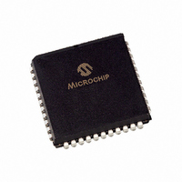
PIC18F452-I/LG Microchip Technology, PIC18F452-I/LG Datasheet - Page 189

PIC18F452-I/LG
Manufacturer Part Number
PIC18F452-I/LG
Description
IC MCU FLASH 16KX16 W/AD 44PLCC
Manufacturer
Microchip Technology
Series
PIC® 18Fr
Datasheets
1.PIC16F616T-ISL.pdf
(8 pages)
2.PIC18F242-ISO.pdf
(332 pages)
3.PIC18F242-ISO.pdf
(14 pages)
4.PIC18F242-ISO.pdf
(16 pages)
5.PIC18F242-ISO.pdf
(16 pages)
6.PIC18F242-ISO.pdf
(14 pages)
7.PIC18LF242-ISO.pdf
(36 pages)
Specifications of PIC18F452-I/LG
Core Processor
PIC
Core Size
8-Bit
Speed
40MHz
Connectivity
I²C, SPI, UART/USART
Peripherals
Brown-out Detect/Reset, LVD, POR, PWM, WDT
Number Of I /o
34
Program Memory Size
32KB (16K x 16)
Program Memory Type
FLASH
Eeprom Size
256 x 8
Ram Size
1.5K x 8
Voltage - Supply (vcc/vdd)
4.2 V ~ 5.5 V
Data Converters
A/D 8x10b
Oscillator Type
External
Operating Temperature
-40°C ~ 85°C
Package / Case
44-PLCC
For Use With
XLT44L2 - SOCKET TRAN ICE 44PLCCDVA16XL441 - ADAPTER DEVICE ICE 44PLCC
Lead Free Status / RoHS Status
Lead free / RoHS Compliant
- PIC16F616T-ISL PDF datasheet
- PIC18F242-ISO PDF datasheet #2
- PIC18F242-ISO PDF datasheet #3
- PIC18F242-ISO PDF datasheet #4
- PIC18F242-ISO PDF datasheet #5
- PIC18F242-ISO PDF datasheet #6
- PIC18LF242-ISO PDF datasheet #7
- Current page: 189 of 332
- Download datasheet (6Mb)
17.4
Figure 17-3 shows the operation of the A/D converter
after the GO bit has been set. Clearing the GO/DONE
bit during a conversion will abort the current conver-
sion. The A/D result register pair will NOT be updated
with the partially completed A/D conversion sample.
That is, the ADRESH:ADRESL registers will continue
to contain the value of the last completed conversion
FIGURE 17-3:
17.4.1
The ADRESH:ADRESL register pair is the location
where the 10-bit A/D result is loaded at the completion
of the A/D conversion. This register pair is 16-bits wide.
The A/D module gives the flexibility to left or right justify
the 10-bit result in the 16-bit result register. The A/D
FIGURE 17-4:
© 2006 Microchip Technology Inc.
A/D Conversions
T
CY
Set GO bit
Holding capacitor is disconnected from analog input (typically 100 ns)
A/D RESULT REGISTERS
- T
AD
7
Conversion Starts
0000 00
ADRESH
T
b9
AD
A/D CONVERSION T
A/D RESULT JUSTIFICATION
1 T
Right Justified
AD
b8
2 1 0 7
ADFM = 1
2 T
AD
b7
10-bit Result
3 T
ADRESL
AD
b6
Next Q4: ADRESH/ADRESL is loaded, GO bit is cleared,
4 T
AD
AD
b5
0
5 T
CYCLES
ADIF bit is set, holding capacitor is connected to analog input.
10-bit Result
AD
b4
6 T
AD
b3
7 T
(or the last value written to the ADRESH:ADRESL reg-
isters). After the A/D conversion is aborted, a 2 T
is required before the next acquisition is started. After
this 2 T
automatically started. The GO/DONE bit can then be
set to start the conversion.
Format Select bit (ADFM) controls this justification.
Figure 17-4 shows the operation of the A/D result justi-
fication. The extra bits are loaded with ’0’s. When an
A/D result will not overwrite these locations (A/D
disable), these registers may be used as two general
purpose 8-bit registers.
Note:
AD
b2
7
8
AD
ADRESH
T
AD
wait, acquisition on the selected channel is
b1
The GO/DONE bit should NOT be set in
the same instruction that turns on the A/D.
10-bit Result
9 T
AD
ADFM = 0
b0
Left Justified
10
0 7 6 5
T
AD
b0
PIC18FXX2
ADRESL
11
0000 00
DS39564C-page 187
0
AD
wait
Related parts for PIC18F452-I/LG
Image
Part Number
Description
Manufacturer
Datasheet
Request
R

Part Number:
Description:
Manufacturer:
Microchip Technology Inc.
Datasheet:

Part Number:
Description:
IC MCU FLASH 16KX16 EE 40DIP
Manufacturer:
Microchip Technology
Datasheet:

Part Number:
Description:
IC MCU FLASH 16KX16 EE 44PLCC
Manufacturer:
Microchip Technology
Datasheet:

Part Number:
Description:
IC MCU FLASH 16KX16 EE 44TQFP
Manufacturer:
Microchip Technology
Datasheet:

Part Number:
Description:
IC MCU FLASH 16KX16 A/D 44QFN
Manufacturer:
Microchip Technology
Datasheet:

Part Number:
Description:
IC MCU CMOS 40MHZ 16K FLSH44TQFP
Manufacturer:
Microchip Technology
Datasheet:

Part Number:
Description:
IC MCU FLASH 16KX16 W/AD 40DIP
Manufacturer:
Microchip Technology
Datasheet:

Part Number:
Description:
IC MCU CMOS 40MHZ 16K FLSH 40DIP
Manufacturer:
Microchip Technology
Datasheet:

Part Number:
Description:
IC MCU CMOS 40MHZ 16K FLSH44PLCC
Manufacturer:
Microchip Technology
Datasheet:

Part Number:
Description:
44 PIN, 32KB ENH FLASH, 1536 RAM, 34 I/O,
Manufacturer:
Microchip Technology
Datasheet:

Part Number:
Description:
PIC18F With 128-segment LCD Driver And 12-bit ADC, 8KB Flash, 768B RAM, CCP, MSS
Manufacturer:
Microchip Technology
Datasheet:

Part Number:
Description:
PIC18F With 128-segment LCD Driver And 12-bit ADC, 16KB Flash, 768B RAM, CCP, MS
Manufacturer:
Microchip Technology
Datasheet:

Part Number:
Description:
PIC18F With 192-segment LCD Driver And 12-bit ADC, 8KB Flash, 768B RAM, CCP, MSS
Manufacturer:
Microchip Technology
Datasheet:

Part Number:
Description:
PIC18F With 192-segment LCD Driver And 12-bit ADC, 16KB Flash, 768B RAM, CCP, MS
Manufacturer:
Microchip Technology
Datasheet:


