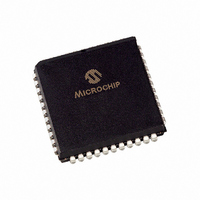
PIC18F452-I/LG Microchip Technology, PIC18F452-I/LG Datasheet - Page 110

PIC18F452-I/LG
Manufacturer Part Number
PIC18F452-I/LG
Description
IC MCU FLASH 16KX16 W/AD 44PLCC
Manufacturer
Microchip Technology
Series
PIC® 18Fr
Datasheets
1.PIC16F616T-ISL.pdf
(8 pages)
2.PIC18F242-ISO.pdf
(332 pages)
3.PIC18F242-ISO.pdf
(14 pages)
4.PIC18F242-ISO.pdf
(16 pages)
5.PIC18F242-ISO.pdf
(16 pages)
6.PIC18F242-ISO.pdf
(14 pages)
7.PIC18LF242-ISO.pdf
(36 pages)
Specifications of PIC18F452-I/LG
Core Processor
PIC
Core Size
8-Bit
Speed
40MHz
Connectivity
I²C, SPI, UART/USART
Peripherals
Brown-out Detect/Reset, LVD, POR, PWM, WDT
Number Of I /o
34
Program Memory Size
32KB (16K x 16)
Program Memory Type
FLASH
Eeprom Size
256 x 8
Ram Size
1.5K x 8
Voltage - Supply (vcc/vdd)
4.2 V ~ 5.5 V
Data Converters
A/D 8x10b
Oscillator Type
External
Operating Temperature
-40°C ~ 85°C
Package / Case
44-PLCC
For Use With
XLT44L2 - SOCKET TRAN ICE 44PLCCDVA16XL441 - ADAPTER DEVICE ICE 44PLCC
Lead Free Status / RoHS Status
Lead free / RoHS Compliant
- PIC16F616T-ISL PDF datasheet
- PIC18F242-ISO PDF datasheet #2
- PIC18F242-ISO PDF datasheet #3
- PIC18F242-ISO PDF datasheet #4
- PIC18F242-ISO PDF datasheet #5
- PIC18F242-ISO PDF datasheet #6
- PIC18LF242-ISO PDF datasheet #7
- Current page: 110 of 332
- Download datasheet (6Mb)
PIC18FXX2
11.1
Timer1 can operate in one of these modes:
• As a timer
• As a synchronous counter
• As an asynchronous counter
The Operating mode is determined by the clock select
bit, TMR1CS (T1CON<1>).
FIGURE 11-1:
FIGURE 11-2:
DS39564C-page 108
T13CKI/T1OSO
Note 1: When enable bit T1OSCEN is cleared, the inverter and feedback resistor are turned off. This eliminates power drain.
Note 1: When enable bit T1OSCEN is cleared, the inverter and feedback resistor are turned off. This eliminates power drain.
T1CKI/T1OSO
T1OSI
TMR1IF
Overflow
Interrupt
Flag bit
Data Bus<7:0>
Timer1 Operation
Write TMR1L
Read TMR1L
TMR1IF
Overflow
Interrupt
Flag Bit
T1OSI
TIMER1 BLOCK DIAGRAM: 16-BIT READ/WRITE MODE
TIMER1 BLOCK DIAGRAM
8
T1OSC
High Byte
TMR1H
Timer 1
8
TMR1H
T1OSC
8
TMR1
TMR1
Oscillator
Enable
T1OSCEN
T1OSCEN
Enable
Oscillator
TMR1L
TMR1L
8
(1)
CLR
(1)
CLR
Clock
Internal
F
OSC
Clock
F
Internal
OSC
/4
TMR1ON
CCP Special Event Trigger
On/Off
/4
TMR1CS
TMR1ON
CCP Special Event Trigger
on/off
1
0
When TMR1CS = 0, Timer1 increments every instruc-
tion cycle. When TMR1CS = 1, Timer1 increments on
every rising edge of the external clock input or the
Timer1 oscillator, if enabled.
When the Timer1 oscillator is enabled (T1OSCEN is
set), the RC1/T1OSI and RC0/T1OSO/T1CKI pins
become inputs. That is, the TRISC<1:0> value is
ignored, and the pins are read as ‘0’.
Timer1 also has an internal “RESET input”. This
RESET can be generated by the CCP module
(Section 14.0).
TMR1CS
1
0
T1CKPS1:T1CKPS0
T1SYNC
Prescaler
1, 2, 4, 8
T1CKPS1:T1CKPS0
T1SYNC
Prescaler
0
1
1, 2, 4, 8
2
1
0
2
© 2006 Microchip Technology Inc.
Synchronized
Clock Input
Synchronize
SLEEP Input
Synchronized
Clock Input
Synchronize
SLEEP Input
det
det
Related parts for PIC18F452-I/LG
Image
Part Number
Description
Manufacturer
Datasheet
Request
R

Part Number:
Description:
Manufacturer:
Microchip Technology Inc.
Datasheet:

Part Number:
Description:
IC MCU FLASH 16KX16 EE 40DIP
Manufacturer:
Microchip Technology
Datasheet:

Part Number:
Description:
IC MCU FLASH 16KX16 EE 44PLCC
Manufacturer:
Microchip Technology
Datasheet:

Part Number:
Description:
IC MCU FLASH 16KX16 EE 44TQFP
Manufacturer:
Microchip Technology
Datasheet:

Part Number:
Description:
IC MCU FLASH 16KX16 A/D 44QFN
Manufacturer:
Microchip Technology
Datasheet:

Part Number:
Description:
IC MCU CMOS 40MHZ 16K FLSH44TQFP
Manufacturer:
Microchip Technology
Datasheet:

Part Number:
Description:
IC MCU FLASH 16KX16 W/AD 40DIP
Manufacturer:
Microchip Technology
Datasheet:

Part Number:
Description:
IC MCU CMOS 40MHZ 16K FLSH 40DIP
Manufacturer:
Microchip Technology
Datasheet:

Part Number:
Description:
IC MCU CMOS 40MHZ 16K FLSH44PLCC
Manufacturer:
Microchip Technology
Datasheet:

Part Number:
Description:
44 PIN, 32KB ENH FLASH, 1536 RAM, 34 I/O,
Manufacturer:
Microchip Technology
Datasheet:

Part Number:
Description:
PIC18F With 128-segment LCD Driver And 12-bit ADC, 8KB Flash, 768B RAM, CCP, MSS
Manufacturer:
Microchip Technology
Datasheet:

Part Number:
Description:
PIC18F With 128-segment LCD Driver And 12-bit ADC, 16KB Flash, 768B RAM, CCP, MS
Manufacturer:
Microchip Technology
Datasheet:

Part Number:
Description:
PIC18F With 192-segment LCD Driver And 12-bit ADC, 8KB Flash, 768B RAM, CCP, MSS
Manufacturer:
Microchip Technology
Datasheet:

Part Number:
Description:
PIC18F With 192-segment LCD Driver And 12-bit ADC, 16KB Flash, 768B RAM, CCP, MS
Manufacturer:
Microchip Technology
Datasheet:


