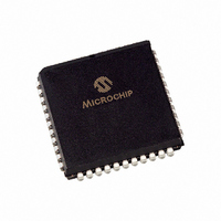
PIC18F452-I/LG Microchip Technology, PIC18F452-I/LG Datasheet - Page 248

PIC18F452-I/LG
Manufacturer Part Number
PIC18F452-I/LG
Description
IC MCU FLASH 16KX16 W/AD 44PLCC
Manufacturer
Microchip Technology
Series
PIC® 18Fr
Datasheets
1.PIC16F616T-ISL.pdf
(8 pages)
2.PIC18F242-ISO.pdf
(332 pages)
3.PIC18F242-ISO.pdf
(14 pages)
4.PIC18F242-ISO.pdf
(16 pages)
5.PIC18F242-ISO.pdf
(16 pages)
6.PIC18F242-ISO.pdf
(14 pages)
7.PIC18LF242-ISO.pdf
(36 pages)
Specifications of PIC18F452-I/LG
Core Processor
PIC
Core Size
8-Bit
Speed
40MHz
Connectivity
I²C, SPI, UART/USART
Peripherals
Brown-out Detect/Reset, LVD, POR, PWM, WDT
Number Of I /o
34
Program Memory Size
32KB (16K x 16)
Program Memory Type
FLASH
Eeprom Size
256 x 8
Ram Size
1.5K x 8
Voltage - Supply (vcc/vdd)
4.2 V ~ 5.5 V
Data Converters
A/D 8x10b
Oscillator Type
External
Operating Temperature
-40°C ~ 85°C
Package / Case
44-PLCC
For Use With
XLT44L2 - SOCKET TRAN ICE 44PLCCDVA16XL441 - ADAPTER DEVICE ICE 44PLCC
Lead Free Status / RoHS Status
Lead free / RoHS Compliant
- PIC16F616T-ISL PDF datasheet
- PIC18F242-ISO PDF datasheet #2
- PIC18F242-ISO PDF datasheet #3
- PIC18F242-ISO PDF datasheet #4
- PIC18F242-ISO PDF datasheet #5
- PIC18F242-ISO PDF datasheet #6
- PIC18LF242-ISO PDF datasheet #7
- Current page: 248 of 332
- Download datasheet (6Mb)
PIC18FXX2
SLEEP
Syntax:
Operands:
Operation:
Status Affected:
Encoding:
Description:
Words:
Cycles:
Example:
† If WDT causes wake-up, this bit is cleared.
DS39564C-page 246
Q Cycle Activity:
Before Instruction
After Instruction
Decode
TO =
PD =
TO =
PD =
Q1
?
?
1 †
0
operation
Enter SLEEP mode
[ label ] SLEEP
None
00h
0
1
0
TO, PD
The power-down status bit (PD) is
cleared. The time-out status bit
(TO) is set. Watchdog Timer and
its postscaler are cleared.
The processor is put into SLEEP
mode with the oscillator stopped.
1
1
SLEEP
No
Q2
0000
WDT postscaler,
TO,
PD
WDT,
0000
Process
Data
Q3
0000
Go to
sleep
Q4
0011
SUBFWB
Syntax:
Operands:
Operation:
Status Affected:
Encoding:
Description:
Words:
Cycles:
Example 1:
Example 2:
Example 3:
Q Cycle Activity:
Before Instruction
After Instruction
Before Instruction
After Instruction
Before Instruction
After Instruction
Decode
REG
W
C
REG
W
C
Z
N
REG
W
C
REG
W
C
Z
N
REG
W
C
REG
W
C
Z
N
Q1
=
=
=
=
=
=
=
=
=
=
=
=
=
=
=
=
=
=
=
=
=
=
=
=
register 'f'
(W) – (f) – (C)
N, OV, C, DC, Z
Subtract f from W with borrow
[ label ] SUBFWB
0
d
a
Subtract register 'f' and carry flag
(borrow) from W (2’s complement
method). If 'd' is 0, the result is
stored in W. If 'd' is 1, the result is
stored in register 'f' (default). If ’a’ is
0, the Access Bank will be selected,
overriding the BSR value. If ’a’ is 1,
then the bank will be selected as
per the BSR value (default).
1
1
SUBFWB
SUBFWB
SUBFWB
Read
Q2
0101
3
2
1
FF
2
0
0
1
2
5
1
2
3
1
0
0
1
2
0
0
2
1
1
0
© 2006 Microchip Technology Inc.
f
[0,1]
[0,1]
; result is negative
; result is positive
; result is zero
255
01da
REG, 1, 0
REG, 0, 0
REG, 1, 0
Process
Data
Q3
dest
ffff
f [,d [,a]
destination
Write to
Q4
ffff
Related parts for PIC18F452-I/LG
Image
Part Number
Description
Manufacturer
Datasheet
Request
R

Part Number:
Description:
Manufacturer:
Microchip Technology Inc.
Datasheet:

Part Number:
Description:
IC MCU FLASH 16KX16 EE 40DIP
Manufacturer:
Microchip Technology
Datasheet:

Part Number:
Description:
IC MCU FLASH 16KX16 EE 44PLCC
Manufacturer:
Microchip Technology
Datasheet:

Part Number:
Description:
IC MCU FLASH 16KX16 EE 44TQFP
Manufacturer:
Microchip Technology
Datasheet:

Part Number:
Description:
IC MCU FLASH 16KX16 A/D 44QFN
Manufacturer:
Microchip Technology
Datasheet:

Part Number:
Description:
IC MCU CMOS 40MHZ 16K FLSH44TQFP
Manufacturer:
Microchip Technology
Datasheet:

Part Number:
Description:
IC MCU FLASH 16KX16 W/AD 40DIP
Manufacturer:
Microchip Technology
Datasheet:

Part Number:
Description:
IC MCU CMOS 40MHZ 16K FLSH 40DIP
Manufacturer:
Microchip Technology
Datasheet:

Part Number:
Description:
IC MCU CMOS 40MHZ 16K FLSH44PLCC
Manufacturer:
Microchip Technology
Datasheet:

Part Number:
Description:
44 PIN, 32KB ENH FLASH, 1536 RAM, 34 I/O,
Manufacturer:
Microchip Technology
Datasheet:

Part Number:
Description:
PIC18F With 128-segment LCD Driver And 12-bit ADC, 8KB Flash, 768B RAM, CCP, MSS
Manufacturer:
Microchip Technology
Datasheet:

Part Number:
Description:
PIC18F With 128-segment LCD Driver And 12-bit ADC, 16KB Flash, 768B RAM, CCP, MS
Manufacturer:
Microchip Technology
Datasheet:

Part Number:
Description:
PIC18F With 192-segment LCD Driver And 12-bit ADC, 8KB Flash, 768B RAM, CCP, MSS
Manufacturer:
Microchip Technology
Datasheet:

Part Number:
Description:
PIC18F With 192-segment LCD Driver And 12-bit ADC, 16KB Flash, 768B RAM, CCP, MS
Manufacturer:
Microchip Technology
Datasheet:


