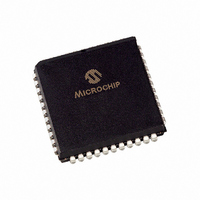
PIC18F452-I/LG Microchip Technology, PIC18F452-I/LG Datasheet - Page 63

PIC18F452-I/LG
Manufacturer Part Number
PIC18F452-I/LG
Description
IC MCU FLASH 16KX16 W/AD 44PLCC
Manufacturer
Microchip Technology
Series
PIC® 18Fr
Datasheets
1.PIC16F616T-ISL.pdf
(8 pages)
2.PIC18F242-ISO.pdf
(332 pages)
3.PIC18F242-ISO.pdf
(14 pages)
4.PIC18F242-ISO.pdf
(16 pages)
5.PIC18F242-ISO.pdf
(16 pages)
6.PIC18F242-ISO.pdf
(14 pages)
7.PIC18LF242-ISO.pdf
(36 pages)
Specifications of PIC18F452-I/LG
Core Processor
PIC
Core Size
8-Bit
Speed
40MHz
Connectivity
I²C, SPI, UART/USART
Peripherals
Brown-out Detect/Reset, LVD, POR, PWM, WDT
Number Of I /o
34
Program Memory Size
32KB (16K x 16)
Program Memory Type
FLASH
Eeprom Size
256 x 8
Ram Size
1.5K x 8
Voltage - Supply (vcc/vdd)
4.2 V ~ 5.5 V
Data Converters
A/D 8x10b
Oscillator Type
External
Operating Temperature
-40°C ~ 85°C
Package / Case
44-PLCC
For Use With
XLT44L2 - SOCKET TRAN ICE 44PLCCDVA16XL441 - ADAPTER DEVICE ICE 44PLCC
Lead Free Status / RoHS Status
Lead free / RoHS Compliant
- PIC16F616T-ISL PDF datasheet
- PIC18F242-ISO PDF datasheet #2
- PIC18F242-ISO PDF datasheet #3
- PIC18F242-ISO PDF datasheet #4
- PIC18F242-ISO PDF datasheet #5
- PIC18F242-ISO PDF datasheet #6
- PIC18LF242-ISO PDF datasheet #7
- Current page: 63 of 332
- Download datasheet (6Mb)
5.5
The minimum programming block is 4 words or 8 bytes.
Word or byte programming is not supported.
Table Writes are used internally to load the holding reg-
isters needed to program the FLASH memory. There
are 8 holding registers used by the Table Writes for
programming.
Since the Table Latch (TABLAT) is only a single byte,
the TBLWT instruction has to be executed 8 times for
each programming operation. All of the Table Write
FIGURE 5-5:
5.5.1
The sequence of events for programming an internal
program memory location should be:
1.
2.
3.
4.
5.
6.
7.
8.
9.
© 2006 Microchip Technology Inc.
TBLPTR = xxxxx0
Read 64 bytes into RAM.
Update data values in RAM as necessary.
Load Table Pointer with address being erased.
Do the row erase procedure.
Load Table Pointer with address of first byte
being written.
Write the first 8 bytes into the holding registers
with auto-increment (TBLWT*+ or TBLWT+*).
Set EEPGD bit to point to program memory,
clear the CFGS bit to access program memory,
and set WREN to enable byte writes.
Disable interrupts.
Write 55h to EECON2.
Writing to FLASH Program
Memory
FLASH PROGRAM MEMORY WRITE
SEQUENCE
Holding Register
8
TABLE WRITES TO FLASH PROGRAM MEMORY
TBLPTR = xxxxx1
Holding Register
8
Program Memory
TBLPTR = xxxxx2
Write Register
TABLAT
operations will essentially be short writes, because only
the holding registers are written. At the end of updating
8 registers, the EECON1 register must be written to, to
start the programming operation with a long write.
The long write is necessary for programming the inter-
nal FLASH. Instruction execution is halted while in a
long write cycle. The long write will be terminated by
the internal programming timer.
The EEPROM on-chip timer controls the write time.
The write/erase voltages are generated by an on-chip
charge pump rated to operate over the voltage range of
the device for byte or word operations.
10. Write AAh to EECON2.
11. Set the WR bit. This will begin the write cycle.
12. The CPU will stall for duration of the write (about
13. Re-enable interrupts.
14. Repeat steps 6-14 seven times, to write
15. Verify the memory (Table Read).
This procedure will require about 18 ms to update one
row of 64 bytes of memory. An example of the required
code is given in Example 5-3.
Note:
Holding Register
2 ms using internal timer).
64 bytes.
8
Before setting the WR bit, the table pointer
address needs to be within the intended
address range of the 8 bytes in the holding
registers.
TBLPTR = xxxxx7
PIC18FXX2
Holding Register
DS39564C-page 61
8
Related parts for PIC18F452-I/LG
Image
Part Number
Description
Manufacturer
Datasheet
Request
R

Part Number:
Description:
Manufacturer:
Microchip Technology Inc.
Datasheet:

Part Number:
Description:
IC MCU FLASH 16KX16 EE 40DIP
Manufacturer:
Microchip Technology
Datasheet:

Part Number:
Description:
IC MCU FLASH 16KX16 EE 44PLCC
Manufacturer:
Microchip Technology
Datasheet:

Part Number:
Description:
IC MCU FLASH 16KX16 EE 44TQFP
Manufacturer:
Microchip Technology
Datasheet:

Part Number:
Description:
IC MCU FLASH 16KX16 A/D 44QFN
Manufacturer:
Microchip Technology
Datasheet:

Part Number:
Description:
IC MCU CMOS 40MHZ 16K FLSH44TQFP
Manufacturer:
Microchip Technology
Datasheet:

Part Number:
Description:
IC MCU FLASH 16KX16 W/AD 40DIP
Manufacturer:
Microchip Technology
Datasheet:

Part Number:
Description:
IC MCU CMOS 40MHZ 16K FLSH 40DIP
Manufacturer:
Microchip Technology
Datasheet:

Part Number:
Description:
IC MCU CMOS 40MHZ 16K FLSH44PLCC
Manufacturer:
Microchip Technology
Datasheet:

Part Number:
Description:
44 PIN, 32KB ENH FLASH, 1536 RAM, 34 I/O,
Manufacturer:
Microchip Technology
Datasheet:

Part Number:
Description:
PIC18F With 128-segment LCD Driver And 12-bit ADC, 8KB Flash, 768B RAM, CCP, MSS
Manufacturer:
Microchip Technology
Datasheet:

Part Number:
Description:
PIC18F With 128-segment LCD Driver And 12-bit ADC, 16KB Flash, 768B RAM, CCP, MS
Manufacturer:
Microchip Technology
Datasheet:

Part Number:
Description:
PIC18F With 192-segment LCD Driver And 12-bit ADC, 8KB Flash, 768B RAM, CCP, MSS
Manufacturer:
Microchip Technology
Datasheet:

Part Number:
Description:
PIC18F With 192-segment LCD Driver And 12-bit ADC, 16KB Flash, 768B RAM, CCP, MS
Manufacturer:
Microchip Technology
Datasheet:


