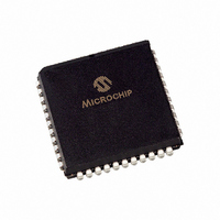
PIC18F452-I/LG Microchip Technology, PIC18F452-I/LG Datasheet - Page 263

PIC18F452-I/LG
Manufacturer Part Number
PIC18F452-I/LG
Description
IC MCU FLASH 16KX16 W/AD 44PLCC
Manufacturer
Microchip Technology
Series
PIC® 18Fr
Datasheets
1.PIC16F616T-ISL.pdf
(8 pages)
2.PIC18F242-ISO.pdf
(332 pages)
3.PIC18F242-ISO.pdf
(14 pages)
4.PIC18F242-ISO.pdf
(16 pages)
5.PIC18F242-ISO.pdf
(16 pages)
6.PIC18F242-ISO.pdf
(14 pages)
7.PIC18LF242-ISO.pdf
(36 pages)
Specifications of PIC18F452-I/LG
Core Processor
PIC
Core Size
8-Bit
Speed
40MHz
Connectivity
I²C, SPI, UART/USART
Peripherals
Brown-out Detect/Reset, LVD, POR, PWM, WDT
Number Of I /o
34
Program Memory Size
32KB (16K x 16)
Program Memory Type
FLASH
Eeprom Size
256 x 8
Ram Size
1.5K x 8
Voltage - Supply (vcc/vdd)
4.2 V ~ 5.5 V
Data Converters
A/D 8x10b
Oscillator Type
External
Operating Temperature
-40°C ~ 85°C
Package / Case
44-PLCC
For Use With
XLT44L2 - SOCKET TRAN ICE 44PLCCDVA16XL441 - ADAPTER DEVICE ICE 44PLCC
Lead Free Status / RoHS Status
Lead free / RoHS Compliant
- PIC16F616T-ISL PDF datasheet
- PIC18F242-ISO PDF datasheet #2
- PIC18F242-ISO PDF datasheet #3
- PIC18F242-ISO PDF datasheet #4
- PIC18F242-ISO PDF datasheet #5
- PIC18F242-ISO PDF datasheet #6
- PIC18LF242-ISO PDF datasheet #7
- Current page: 263 of 332
- Download datasheet (6Mb)
22.1
© 2006 Microchip Technology Inc.
PIC18LFXX2
PIC18FXX2
D001
D001
D002
D003
D004
D005
D005
Legend: Shading of rows is to assist in readability of the table.
Note 1: This is the limit to which V
Param
No.
(Industrial)
(Industrial, Extended)
2: The supply current is mainly a function of the operating voltage and frequency. Other factors, such as I/O pin
3: The power-down current in SLEEP mode does not depend on the oscillator type. Power-down current is
4: For RC osc configuration, current through R
5: The LVD and BOR modules share a large portion of circuitry. The I
DC Characteristics: PIC18FXX2 (Industrial, Extended)
V
V
V
S
V
Symbol
loading and switching rate, oscillator type, internal code execution pattern and temperature, also have an
impact on the current consumption.
The test conditions for all I
measured with the part in SLEEP mode, with all I/O pins in hi-impedance state and tied to V
features that add delta current disabled (such as WDT, Timer1 Oscillator, BOR,...).
estimated by the formula Ir = V
Once one of these modules is enabled, the other may also be enabled without further penalty.
DD
DR
POR
VDD
BOR
Supply Voltage
RAM Data Retention
Voltage
V
to ensure internal
Power-on Reset signal
V
to ensure internal
Power-on Reset signal
Brown-out Reset Voltage
DD
DD
OSC1 = external square wave, from rail-to-rail; all I/O pins tri-stated, pulled to V
MCLR = V
BORV1:BORV0 = 11
BORV1:BORV0 = 10
BORV1:BORV0 = 01
BORV1:BORV0 = 00
BORV1:BORV0 = 1x
BORV1:BORV0 = 01
BORV1:BORV0 = 00
Characteristic
Start Voltage
Rise Rate
(1)
PIC18LFXX2
PIC18LFXX2
PIC18FXX2
PIC18FXX2
DD
; WDT enabled/disabled as specified.
DD
PIC18LFXX2 (Industrial)
DD
can be lowered in SLEEP mode, or during a device RESET, without losing RAM data.
measurements in active Operation mode are:
DD
/2R
Standard Operating Conditions (unless otherwise stated)
Operating temperature
Standard Operating Conditions (unless otherwise stated)
Operating temperature
0.05
1.98
2.67
4.16
4.45
N.A.
4.16
4.45
Min
2.0
4.2
1.5
—
EXT
(mA) with R
Typ
—
—
—
—
—
—
—
—
—
—
—
—
EXT
is not included. The current through the resistor can be
Max Units
2.14
2.89
4.83
N.A.
4.83
5.5
5.5
0.7
4.5
4.5
—
—
EXT
V/ms See Section 3.1 (Power-on Reset) for details
V
V
V
V
V
V
V
V
V
V
V
in kOhm.
-40°C
-40°C
-40°C
HS, XT, RC and LP Osc mode
See Section 3.1 (Power-on Reset) for details
85 C
Not in operating voltage range of device
BOR
T
T
T
T
A
A
A
and I
25 C
+85°C for industrial
+85°C for industrial
+125°C for extended
PIC18FXX2
LVD
Conditions
currents are not additive.
DS39564C-page 261
DD
DD
or V
SS
, and all
Related parts for PIC18F452-I/LG
Image
Part Number
Description
Manufacturer
Datasheet
Request
R

Part Number:
Description:
Manufacturer:
Microchip Technology Inc.
Datasheet:

Part Number:
Description:
IC MCU FLASH 16KX16 EE 40DIP
Manufacturer:
Microchip Technology
Datasheet:

Part Number:
Description:
IC MCU FLASH 16KX16 EE 44PLCC
Manufacturer:
Microchip Technology
Datasheet:

Part Number:
Description:
IC MCU FLASH 16KX16 EE 44TQFP
Manufacturer:
Microchip Technology
Datasheet:

Part Number:
Description:
IC MCU FLASH 16KX16 A/D 44QFN
Manufacturer:
Microchip Technology
Datasheet:

Part Number:
Description:
IC MCU CMOS 40MHZ 16K FLSH44TQFP
Manufacturer:
Microchip Technology
Datasheet:

Part Number:
Description:
IC MCU FLASH 16KX16 W/AD 40DIP
Manufacturer:
Microchip Technology
Datasheet:

Part Number:
Description:
IC MCU CMOS 40MHZ 16K FLSH 40DIP
Manufacturer:
Microchip Technology
Datasheet:

Part Number:
Description:
IC MCU CMOS 40MHZ 16K FLSH44PLCC
Manufacturer:
Microchip Technology
Datasheet:

Part Number:
Description:
44 PIN, 32KB ENH FLASH, 1536 RAM, 34 I/O,
Manufacturer:
Microchip Technology
Datasheet:

Part Number:
Description:
PIC18F With 128-segment LCD Driver And 12-bit ADC, 8KB Flash, 768B RAM, CCP, MSS
Manufacturer:
Microchip Technology
Datasheet:

Part Number:
Description:
PIC18F With 128-segment LCD Driver And 12-bit ADC, 16KB Flash, 768B RAM, CCP, MS
Manufacturer:
Microchip Technology
Datasheet:

Part Number:
Description:
PIC18F With 192-segment LCD Driver And 12-bit ADC, 8KB Flash, 768B RAM, CCP, MSS
Manufacturer:
Microchip Technology
Datasheet:

Part Number:
Description:
PIC18F With 192-segment LCD Driver And 12-bit ADC, 16KB Flash, 768B RAM, CCP, MS
Manufacturer:
Microchip Technology
Datasheet:


