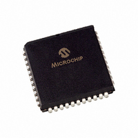
PIC18F452-I/LG Microchip Technology, PIC18F452-I/LG Datasheet - Page 289

PIC18F452-I/LG
Manufacturer Part Number
PIC18F452-I/LG
Description
IC MCU FLASH 16KX16 W/AD 44PLCC
Manufacturer
Microchip Technology
Series
PIC® 18Fr
Datasheets
1.PIC16F616T-ISL.pdf
(8 pages)
2.PIC18F242-ISO.pdf
(332 pages)
3.PIC18F242-ISO.pdf
(14 pages)
4.PIC18F242-ISO.pdf
(16 pages)
5.PIC18F242-ISO.pdf
(16 pages)
6.PIC18F242-ISO.pdf
(14 pages)
7.PIC18LF242-ISO.pdf
(36 pages)
Specifications of PIC18F452-I/LG
Core Processor
PIC
Core Size
8-Bit
Speed
40MHz
Connectivity
I²C, SPI, UART/USART
Peripherals
Brown-out Detect/Reset, LVD, POR, PWM, WDT
Number Of I /o
34
Program Memory Size
32KB (16K x 16)
Program Memory Type
FLASH
Eeprom Size
256 x 8
Ram Size
1.5K x 8
Voltage - Supply (vcc/vdd)
4.2 V ~ 5.5 V
Data Converters
A/D 8x10b
Oscillator Type
External
Operating Temperature
-40°C ~ 85°C
Package / Case
44-PLCC
For Use With
XLT44L2 - SOCKET TRAN ICE 44PLCCDVA16XL441 - ADAPTER DEVICE ICE 44PLCC
Lead Free Status / RoHS Status
Lead free / RoHS Compliant
- PIC16F616T-ISL PDF datasheet
- PIC18F242-ISO PDF datasheet #2
- PIC18F242-ISO PDF datasheet #3
- PIC18F242-ISO PDF datasheet #4
- PIC18F242-ISO PDF datasheet #5
- PIC18F242-ISO PDF datasheet #6
- PIC18LF242-ISO PDF datasheet #7
- Current page: 289 of 332
- Download datasheet (6Mb)
TABLE 22-21: A/D CONVERTER CHARACTERISTICS: PIC18FXX2 (INDUSTRIAL, EXTENDED)
FIGURE 22-22:
© 2006 Microchip Technology Inc.
A01
A03
A04
A05
A06
A10
A20
A20A
A21
A22
A25
A30
A50
Param
No.
Note 1: Vss
Note 1: If the A/D clock source is selected as RC, a time of T
A/D DATA
SAMPLE
N
E
E
E
E
—
V
V
V
V
Z
I
A/D CLK
Symbol
REF
2: The A/D conversion result never decreases with an increase in the Input Voltage, and has no missing codes.
3: For V
4: Maximum allowed impedance for analog voltage source is 10 k . This requires higher acquisition times.
ADRES
2: This is a minimal RC delay (typically 100 nS), which also disconnects the holding capacitor from the analog input.
AIN
REF
REFH
REFL
AIN
R
IL
DL
G
OFF
BSF ADCON0, GO
ADIF
This allows the SLEEP instruction to be executed.
GO
Q4
Resolution
Integral linearity error
Differential linearity error
Gain error
Offset error
Monotonicity
Reference Voltage
(V
Reference voltage High
Reference voltage Low
Analog input voltage
Recommended impedance of
analog voltage source
V
DD
V
REF
REFH
AIN
132
< 2.5V, V
A/D CONVERSION TIMING
input current (Note 1)
Characteristic
– V
V
REF
REFL
AIN
(Note 2)
)
should be limited to < .5 V
9
8
OLD_DATA
AV
AV
7
SS
SS
AV
1.8V
Min
3V
—
—
—
—
—
—
—
—
CY
– 0.3V
– 0.3V
SS
is added before the A/D clock starts.
. . .
SAMPLING STOPPED
DD
guaranteed
.
. . .
Typ
131
130
—
—
—
—
—
—
—
—
—
—
—
—
—
PIC18LFXX2 (INDUSTRIAL)
(2)
AV
AV
2
DD
DD
V
<±1.5
Max
<±1
<±1
<±1
150
REFH
2.5
10
—
—
5
+ 0.3V
+ 0.3V
1
Units
LSb V
LSb V
LSb V
LSb V
k
bit
—
V
V
V
V
V
A
A
0
PIC18FXX2
V
V
V
V
(Note 4)
During V
During A/D conversion cycle
REF
REF
REF
REF
SS
DD
DD
DD
< 3.0V
= V
= V
= V
= V
NEW_DATA
DONE
V
3.0V
2.5V (Note 3)
AIN
DS39564C-page 287
Conditions
AIN
DD
DD
DD
DD
T
= 5.0V
= 5.0V
= 5.0V
= 5.0V
acquisition
CY
V
REF
Related parts for PIC18F452-I/LG
Image
Part Number
Description
Manufacturer
Datasheet
Request
R

Part Number:
Description:
Manufacturer:
Microchip Technology Inc.
Datasheet:

Part Number:
Description:
IC MCU FLASH 16KX16 EE 40DIP
Manufacturer:
Microchip Technology
Datasheet:

Part Number:
Description:
IC MCU FLASH 16KX16 EE 44PLCC
Manufacturer:
Microchip Technology
Datasheet:

Part Number:
Description:
IC MCU FLASH 16KX16 EE 44TQFP
Manufacturer:
Microchip Technology
Datasheet:

Part Number:
Description:
IC MCU FLASH 16KX16 A/D 44QFN
Manufacturer:
Microchip Technology
Datasheet:

Part Number:
Description:
IC MCU CMOS 40MHZ 16K FLSH44TQFP
Manufacturer:
Microchip Technology
Datasheet:

Part Number:
Description:
IC MCU FLASH 16KX16 W/AD 40DIP
Manufacturer:
Microchip Technology
Datasheet:

Part Number:
Description:
IC MCU CMOS 40MHZ 16K FLSH 40DIP
Manufacturer:
Microchip Technology
Datasheet:

Part Number:
Description:
IC MCU CMOS 40MHZ 16K FLSH44PLCC
Manufacturer:
Microchip Technology
Datasheet:

Part Number:
Description:
44 PIN, 32KB ENH FLASH, 1536 RAM, 34 I/O,
Manufacturer:
Microchip Technology
Datasheet:

Part Number:
Description:
PIC18F With 128-segment LCD Driver And 12-bit ADC, 8KB Flash, 768B RAM, CCP, MSS
Manufacturer:
Microchip Technology
Datasheet:

Part Number:
Description:
PIC18F With 128-segment LCD Driver And 12-bit ADC, 16KB Flash, 768B RAM, CCP, MS
Manufacturer:
Microchip Technology
Datasheet:

Part Number:
Description:
PIC18F With 192-segment LCD Driver And 12-bit ADC, 8KB Flash, 768B RAM, CCP, MSS
Manufacturer:
Microchip Technology
Datasheet:

Part Number:
Description:
PIC18F With 192-segment LCD Driver And 12-bit ADC, 16KB Flash, 768B RAM, CCP, MS
Manufacturer:
Microchip Technology
Datasheet:


