MC56F8006DEMO Freescale Semiconductor, MC56F8006DEMO Datasheet - Page 33
MC56F8006DEMO
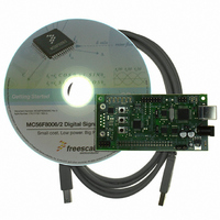
Manufacturer Part Number
MC56F8006DEMO
Description
DEMO BOARD FOR MC56F8006
Manufacturer
Freescale Semiconductor
Type
DSPr
Datasheets
1.MC56F8006DEMO.pdf
(13 pages)
2.MC56F8006DEMO.pdf
(8 pages)
3.MC56F8006DEMO.pdf
(2 pages)
4.MC56F8006DEMO.pdf
(100 pages)
Specifications of MC56F8006DEMO
Contents
Board
Processor To Be Evaluated
MC56F8006
Interface Type
RS-232, USB
Operating Supply Voltage
3.3 V
Silicon Manufacturer
Freescale
Core Architecture
56800/E
Core Sub-architecture
56800/E
Silicon Core Number
MC56F
Silicon Family Name
MC56F80xx
Rohs Compliant
Yes
For Use With/related Products
MC56F8006
Lead Free Status / RoHS Status
Lead free / RoHS Compliant


6
6.1
This section discusses power pins, reset sources, interrupt sources, clock sources, the system integration module (SIM), ADC
synchronization, and JTAG/EOnCE interfaces.
6.2
V
peripherals, I/O buffer circuitry and to internal voltage regulators. Device has multiple internal voltages provide regulated
lower-voltage source for the peripherals, core, memory, and on-chip relaxation oscillators.
Typically, there are at least two separate capacitors across the power pins to bypass the glitches and provide bulk charge storage.
In this case, there should be a bulk electrolytic or tantalum capacitor, such as a 10 F tantalum capacitor, to provide bulk charge
storage for the overall system and a 0.1 F ceramic bypass capacitor located as near to the device power pins as practical to
suppress high-frequency noise. Each pin must have a bypass capacitor for best noise suppression.
V
CMP modules. A 0.1 F ceramic bypass capacitor should be located as near to the device V
suppress high-frequency noise. V
respectively, for the ADC module.
6.3
Resetting the device provides a way to start processing from a known set of initial conditions. During reset, most control and
status registers are forced to initial values and the program counter is loaded from the reset vector. On-chip peripheral modules
are disabled and I/O pins are initially configured as the reset status shown in
sources for reset:
Each of these sources has an associated bit in the reset status register (RSTAT) in the system integration module (SIM).
The external pin reset function is shared with an GPIO port A7 on the RESET/GPIOA7 pin. The reset function is enabled
following any reset of the device. Bit 7 of GPIOA_PER register must be cleared to use this pin as an GPIO port pin. When
enabled as the RESET pin, an internal pullup device is automatically enabled.
6.4
The on-chip clock synthesis (OCCS) module allows designers using an internal relaxation oscillator, an external crystal, or an
external clock to run 56F8000 family devices at user-selectable frequencies up to 32 MHz.
The features of OCCS module include:
Freescale Semiconductor
DD
DDA
•
•
•
•
•
•
•
•
•
•
, V
and V
SS
Power-on reset (POR)
Partial power down reset (PPD)
Low-voltage detect (LVD)
External pin reset (EXTR)
Computer operating properly loss of reference reset (COP_LOR)
Computer operating properly time-out reset (COP_CPU)
Software Reset (SWR)
Ability to power down the internal relaxation oscillator or crystal oscillator
Ability to put the internal relaxation oscillator into standby mode
Ability to power down the PLL
and V
General System Control Information
Overview
Power Pins
Reset
On-chip Clock Synthesis
SSA
DDA
are the analog power supply pins for the device. This voltage source supplies power to the ADC, PGA, and
, V
SSA
are the primary power supply pins for the devices. This voltage source supplies power to all on-chip
DDA
MC56F8006/MC56F8002 Digital Signal Controller, Rev. 3
and V
SSA
are also the voltage reference high and voltage reference low inputs,
Table
5. The 56F8006/56F8002 has the following
General System Control Information
DDA
and V
SSA
pins as practical to
33
Related parts for MC56F8006DEMO
Image
Part Number
Description
Manufacturer
Datasheet
Request
R

Part Number:
Description:
Manufacturer:
Freescale Semiconductor, Inc
Datasheet:
Part Number:
Description:
Manufacturer:
Freescale Semiconductor, Inc
Datasheet:
Part Number:
Description:
Manufacturer:
Freescale Semiconductor, Inc
Datasheet:
Part Number:
Description:
Manufacturer:
Freescale Semiconductor, Inc
Datasheet:
Part Number:
Description:
Manufacturer:
Freescale Semiconductor, Inc
Datasheet:
Part Number:
Description:
Manufacturer:
Freescale Semiconductor, Inc
Datasheet:
Part Number:
Description:
Manufacturer:
Freescale Semiconductor, Inc
Datasheet:
Part Number:
Description:
Manufacturer:
Freescale Semiconductor, Inc
Datasheet:
Part Number:
Description:
Manufacturer:
Freescale Semiconductor, Inc
Datasheet:
Part Number:
Description:
Manufacturer:
Freescale Semiconductor, Inc
Datasheet:
Part Number:
Description:
Manufacturer:
Freescale Semiconductor, Inc
Datasheet:
Part Number:
Description:
Manufacturer:
Freescale Semiconductor, Inc
Datasheet:
Part Number:
Description:
Manufacturer:
Freescale Semiconductor, Inc
Datasheet:
Part Number:
Description:
Manufacturer:
Freescale Semiconductor, Inc
Datasheet:
Part Number:
Description:
Manufacturer:
Freescale Semiconductor, Inc
Datasheet: