MC56F8006DEMO Freescale Semiconductor, MC56F8006DEMO Datasheet - Page 19
MC56F8006DEMO
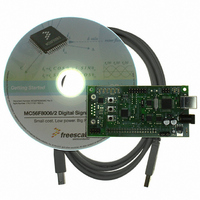
Manufacturer Part Number
MC56F8006DEMO
Description
DEMO BOARD FOR MC56F8006
Manufacturer
Freescale Semiconductor
Type
DSPr
Datasheets
1.MC56F8006DEMO.pdf
(13 pages)
2.MC56F8006DEMO.pdf
(8 pages)
3.MC56F8006DEMO.pdf
(2 pages)
4.MC56F8006DEMO.pdf
(100 pages)
Specifications of MC56F8006DEMO
Contents
Board
Processor To Be Evaluated
MC56F8006
Interface Type
RS-232, USB
Operating Supply Voltage
3.3 V
Silicon Manufacturer
Freescale
Core Architecture
56800/E
Core Sub-architecture
56800/E
Silicon Core Number
MC56F
Silicon Family Name
MC56F80xx
Rohs Compliant
Yes
For Use With/related Products
MC56F8006
Lead Free Status / RoHS Status
Lead free / RoHS Compliant


Freescale Semiconductor
(CLKO_1)
(FAULT0)
(ANA1 &
(ANB13)
GPIOA6
GPIOB0
(PWM3)
(SCLK)
Signal
ANB1)
Name
(SCL)
(TXD)
(SCL)
(T1)
SOIC
28
12
15
LQFP
Table 5. 56F8006/56F8002 Signal and Package Information (continued)
32
18
21
LQFP
48
26
32
MC56F8006/MC56F8002 Digital Signal Controller, Rev. 3
Input/Open
Input/Open
Output
Analog
Output
Output
Output
Output
Output
Output
Analog
Output
Output
Input/
-drain
Input/
Input/
-drain
Input/
Type
Input
Input
Input
enabled
enabled
internal
internal
During
Reset
pullup
pullup
Input,
Input,
State
Port A GPIO — This GPIO pin can be individually programmed as
an input or output pin.
FAULT0 — PWM fault input 0 used for disabling selected PWM
outputs in cases where fault conditions originate off-chip.
ANA1 and ANB1 — Analog input to channel 1 of ADCA and ADCB.
SCL — The I
TXD — The SCI transmit data output or transmit/receive in single
wire operation.
CLKO_1 — This is a buffered clock output; the clock source is
selected by clockout select (CLKOSEL) bits in the clock output
select register (CLKOUT) in the SIM.
When used as an analog input, the signal goes to the ANA1 and
ANB1.
After reset, the default state is GPIOA6.
Port B GPIO — This GPIO pin can be individually programmed as
an input or output pin.
SCLK — The SPI serial clock. In master mode, this pin serves as
an output, clocking slaved listeners. In slave mode, this pin serves
as the data clock input.
SCL — The I
ANB13 — Analog input to channel 13 of ADCB
PWM3 — The PWM channel 3.
T1 — Dual timer module channel 1 input/output.
After reset, the default state is GPIOB0.
2
2
C serial clock
C serial clock.
Signal Description
Signal/Connection Descriptions
19
Related parts for MC56F8006DEMO
Image
Part Number
Description
Manufacturer
Datasheet
Request
R

Part Number:
Description:
Manufacturer:
Freescale Semiconductor, Inc
Datasheet:
Part Number:
Description:
Manufacturer:
Freescale Semiconductor, Inc
Datasheet:
Part Number:
Description:
Manufacturer:
Freescale Semiconductor, Inc
Datasheet:
Part Number:
Description:
Manufacturer:
Freescale Semiconductor, Inc
Datasheet:
Part Number:
Description:
Manufacturer:
Freescale Semiconductor, Inc
Datasheet:
Part Number:
Description:
Manufacturer:
Freescale Semiconductor, Inc
Datasheet:
Part Number:
Description:
Manufacturer:
Freescale Semiconductor, Inc
Datasheet:
Part Number:
Description:
Manufacturer:
Freescale Semiconductor, Inc
Datasheet:
Part Number:
Description:
Manufacturer:
Freescale Semiconductor, Inc
Datasheet:
Part Number:
Description:
Manufacturer:
Freescale Semiconductor, Inc
Datasheet:
Part Number:
Description:
Manufacturer:
Freescale Semiconductor, Inc
Datasheet:
Part Number:
Description:
Manufacturer:
Freescale Semiconductor, Inc
Datasheet:
Part Number:
Description:
Manufacturer:
Freescale Semiconductor, Inc
Datasheet:
Part Number:
Description:
Manufacturer:
Freescale Semiconductor, Inc
Datasheet:
Part Number:
Description:
Manufacturer:
Freescale Semiconductor, Inc
Datasheet: