MC56F8006DEMO Freescale Semiconductor, MC56F8006DEMO Datasheet - Page 25
MC56F8006DEMO
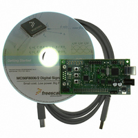
Manufacturer Part Number
MC56F8006DEMO
Description
DEMO BOARD FOR MC56F8006
Manufacturer
Freescale Semiconductor
Type
DSPr
Datasheets
1.MC56F8006DEMO.pdf
(13 pages)
2.MC56F8006DEMO.pdf
(8 pages)
3.MC56F8006DEMO.pdf
(2 pages)
4.MC56F8006DEMO.pdf
(100 pages)
Specifications of MC56F8006DEMO
Contents
Board
Processor To Be Evaluated
MC56F8006
Interface Type
RS-232, USB
Operating Supply Voltage
3.3 V
Silicon Manufacturer
Freescale
Core Architecture
56800/E
Core Sub-architecture
56800/E
Silicon Core Number
MC56F
Silicon Family Name
MC56F80xx
Rohs Compliant
Yes
For Use With/related Products
MC56F8006
Lead Free Status / RoHS Status
Lead free / RoHS Compliant


Freescale Semiconductor
(ANA4 and
CMP1_P2)
(GPIOD0)
(GPIOD1)
(GPIOD2)
(ANB12)
(ANB10)
(CMP0_
(CMP2_
(CMP2_
Signal
(TIN2)
Name
OUT)
OUT)
OUT)
TDO
(SS)
TCK
(T0)
TDI
SOIC
28
23
25
9
LQFP
Table 5. 56F8006/56F8002 Signal and Package Information (continued)
32
30
32
14
LQFP
48
45
48
22
MC56F8006/MC56F8002 Digital Signal Controller, Rev. 3
Output
Analog
Output
Output
Output
Analog
Output
Output
Output
Analog
Output
Input/
Input/
Input/
Input/
Type
Input
Input
Input
Input
Input
Input
Input
tri-stated,
enabled
enabled
enabled
internal
Output,
internal
internal
During
Reset
pullup
pullup
pullup
Input,
Input,
State
Test Data Input — This input pin provides a serial input data stream
to the JTAG/EOnCE port. It is sampled on the rising edge of TCK
and has an on-chip pullup resistor.
Port D GPIO — This GPIO pin can be individually programmed as
an input or output pin.
ANB12 — Analog input to channel 12 of ADCB
SS — SS is used in slave mode to indicate to the SPI module that
the current transfer is to be received.
TIN2 — Dual timer module channel 2 input.
CMP1_OUT — Analog comparator 1 output.
After reset, the default state is TDI.
Test Data Output — This three-stateable output pin provides a serial
output data stream from the JTAG/EOnCE port. It is driven in the
shift-IR and shift-DR controller states, and changes on the falling
edge of TCK.
Port D GPIO — This GPIO pin can be individually programmed as
an input or output pin.
ANB10 — Analog input to channel 10 of ADCB.
T0 — Dual timer module channel 0 input/output.
CMP2_OUT — Analog comparator 2 output.
After reset, the default state is TDO.
Test Clock Input — This input pin provides a gated clock to
synchronize the test logic and shift serial data to the JTAG/EOnCE
port. The pin is connected internally to a pullup resistor. A
Schmitt-trigger input is used for noise immunity.
Port D GPIO — This GPIO pin can be individually programmed as
an input or output pin.
ANA4 and CMP1_P2 — Analog input to channel 4 of ADCA and
positive input 2 of analog comparator 1.
CMP2_OUT — Analog comparator 2 output.
After reset, the default state is TCK.
Signal Description
Signal/Connection Descriptions
25
Related parts for MC56F8006DEMO
Image
Part Number
Description
Manufacturer
Datasheet
Request
R

Part Number:
Description:
Manufacturer:
Freescale Semiconductor, Inc
Datasheet:
Part Number:
Description:
Manufacturer:
Freescale Semiconductor, Inc
Datasheet:
Part Number:
Description:
Manufacturer:
Freescale Semiconductor, Inc
Datasheet:
Part Number:
Description:
Manufacturer:
Freescale Semiconductor, Inc
Datasheet:
Part Number:
Description:
Manufacturer:
Freescale Semiconductor, Inc
Datasheet:
Part Number:
Description:
Manufacturer:
Freescale Semiconductor, Inc
Datasheet:
Part Number:
Description:
Manufacturer:
Freescale Semiconductor, Inc
Datasheet:
Part Number:
Description:
Manufacturer:
Freescale Semiconductor, Inc
Datasheet:
Part Number:
Description:
Manufacturer:
Freescale Semiconductor, Inc
Datasheet:
Part Number:
Description:
Manufacturer:
Freescale Semiconductor, Inc
Datasheet:
Part Number:
Description:
Manufacturer:
Freescale Semiconductor, Inc
Datasheet:
Part Number:
Description:
Manufacturer:
Freescale Semiconductor, Inc
Datasheet:
Part Number:
Description:
Manufacturer:
Freescale Semiconductor, Inc
Datasheet:
Part Number:
Description:
Manufacturer:
Freescale Semiconductor, Inc
Datasheet:
Part Number:
Description:
Manufacturer:
Freescale Semiconductor, Inc
Datasheet: