MC56F8006DEMO Freescale Semiconductor, MC56F8006DEMO Datasheet - Page 18
MC56F8006DEMO
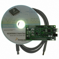
Manufacturer Part Number
MC56F8006DEMO
Description
DEMO BOARD FOR MC56F8006
Manufacturer
Freescale Semiconductor
Type
DSPr
Datasheets
1.MC56F8006DEMO.pdf
(13 pages)
2.MC56F8006DEMO.pdf
(8 pages)
3.MC56F8006DEMO.pdf
(2 pages)
4.MC56F8006DEMO.pdf
(100 pages)
Specifications of MC56F8006DEMO
Contents
Board
Processor To Be Evaluated
MC56F8006
Interface Type
RS-232, USB
Operating Supply Voltage
3.3 V
Silicon Manufacturer
Freescale
Core Architecture
56800/E
Core Sub-architecture
56800/E
Silicon Core Number
MC56F
Silicon Family Name
MC56F80xx
Rohs Compliant
Yes
For Use With/related Products
MC56F8006
Lead Free Status / RoHS Status
Lead free / RoHS Compliant


Signal/Connection Descriptions
EXT_SYNC)
18
(FAULT1)
(FAULT2/
GPIOA3
(PWM3)
(EXTAL)
GPIOA4
(PWM4)
GPIOA5
(PWM5)
Signal
(TIN2)
(TIN3)
Name
(TXD)
(SDA)
SOIC
28
17
16
14
LQFP
Table 5. 56F8006/56F8002 Signal and Package Information (continued)
32
24
22
20
LQFP
48
36
33
29
MC56F8006/MC56F8002 Digital Signal Controller, Rev. 3
Input/Open
Output
Output
Output
Analog
Output
Output
Output
Output
Output
Output
Input/
Input/
-drain
Input/
Input/
Type
Input
Input
Input
Input
enabled
enabled
enabled
internal
internal
internal
During
Reset
pullup
pullup
pullup
Input,
Input,
Input,
State
Port A GPIO — This GPIO pin can be individually programmed as
an input or output pin.
PWM3 — The PWM channel 3.
TXD — The SCI transmit data output or transmit/receive in single
wire operation.
EXTAL — External Crystal Oscillator Input. This input can be
connected to a 32.768 kHz or 1–16 MHz external crystal or ceramic
resonator. When used to supply a source to the internal PLL, the
crystal/resonator must be in the 4 MHz to 8 MHz range. Tie this pin
low or configure as GPIO if XTAL is being driven by an external
clock source.
If using a 32.768 kHz crystal, place the crystal as close as possible
to device pins to speed startup.
After reset, the default state is GPIOA3.
Port A GPIO — This GPIO pin can be individually programmed as
an input or output pin.
PWM4 — The PWM channel 4.
SDA — The I
FAULT1 — PWM fault input 1used for disabling selected PWM
outputs in cases where fault conditions originate off-chip.
TIN2 — Dual timer module channel 2 input
After reset, the default state is GPIOA4.
Port A GPIO — This GPIO pin can be individually programmed as
an input or output pin.
PWM5 — The PWM channel 5.
FAULT2 — PWM fault input 2 used for disabling selected PWM
outputs in cases where fault conditions originate off-chip.
EXT_SYNC — When not being used as a fault input, this pin can be
used to receive a pulse to reset the PWM counter or to generate a
positive pulse at the start of every PWM cycle.
TIN3 — Dual timer module channel 3 input
After reset, the default state is GPIOA5.
2
C serial data line.
Signal Description
Freescale Semiconductor
Related parts for MC56F8006DEMO
Image
Part Number
Description
Manufacturer
Datasheet
Request
R

Part Number:
Description:
Manufacturer:
Freescale Semiconductor, Inc
Datasheet:
Part Number:
Description:
Manufacturer:
Freescale Semiconductor, Inc
Datasheet:
Part Number:
Description:
Manufacturer:
Freescale Semiconductor, Inc
Datasheet:
Part Number:
Description:
Manufacturer:
Freescale Semiconductor, Inc
Datasheet:
Part Number:
Description:
Manufacturer:
Freescale Semiconductor, Inc
Datasheet:
Part Number:
Description:
Manufacturer:
Freescale Semiconductor, Inc
Datasheet:
Part Number:
Description:
Manufacturer:
Freescale Semiconductor, Inc
Datasheet:
Part Number:
Description:
Manufacturer:
Freescale Semiconductor, Inc
Datasheet:
Part Number:
Description:
Manufacturer:
Freescale Semiconductor, Inc
Datasheet:
Part Number:
Description:
Manufacturer:
Freescale Semiconductor, Inc
Datasheet:
Part Number:
Description:
Manufacturer:
Freescale Semiconductor, Inc
Datasheet:
Part Number:
Description:
Manufacturer:
Freescale Semiconductor, Inc
Datasheet:
Part Number:
Description:
Manufacturer:
Freescale Semiconductor, Inc
Datasheet:
Part Number:
Description:
Manufacturer:
Freescale Semiconductor, Inc
Datasheet:
Part Number:
Description:
Manufacturer:
Freescale Semiconductor, Inc
Datasheet: