C8051F800DK Silicon Laboratories Inc, C8051F800DK Datasheet - Page 65
C8051F800DK
Manufacturer Part Number
C8051F800DK
Description
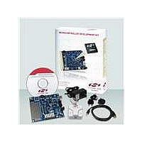
KIT DEV C8051F800
Manufacturer
Silicon Laboratories Inc
Type
MCUr
Specifications of C8051F800DK
Contents
Board, Cables, CD, Debugger, Power Supply
Processor To Be Evaluated
C8051F800
Data Bus Width
16 bit
Interface Type
USB
Operating Supply Voltage
7 V to 15 V
Lead Free Status / RoHS Status
Contains lead / RoHS non-compliant
For Use With/related Products
C8051F8xx
Lead Free Status / Rohs Status
Supplier Unconfirmed
Other names
336-1797


12. Comparator0
C8051F80x-83x devices include an on-chip programmable voltage comparator, Comparator0, shown in
Figure 12.1.
The Comparator offers programmable response time and hysteresis, an analog input multiplexer, and two
outputs that are optionally available at the Port pins: a synchronous “latched” output (CP0), or an asyn-
chronous “raw” output (CP0A). The asynchronous CP0A signal is available even when the system clock is
not active. This allows the Comparator to operate and generate an output with the device in STOP mode.
When assigned to a Port pin, the Comparator output may be configured as open drain or push-pull (see
Section “23.4. Port I/O Initialization” on page 147). Comparator0 may also be used as a reset source (see
Section “21.5. Comparator0 Reset” on page 127).
The Comparator0 inputs are selected by the comparator input multiplexer, as detailed in Section
“12.1. Comparator Multiplexer” on page 69.
The Comparator output can be polled in software, used as an interrupt source, and/or routed to a Port pin.
When routed to a Port pin, the Comparator output is available asynchronous or synchronous to the system
clock; the asynchronous output is available even in STOP mode (with no system clock active). When dis-
abled, the Comparator output (if assigned to a Port I/O pin via the Crossbar) defaults to the logic low state,
and the power supply to the comparator is turned off. See Section “23.3. Priority Crossbar Decoder” on
page 143 for details on configuring Comparator outputs via the digital Crossbar. Comparator inputs can be
externally driven from –0.25 V to (V
trical specifications are given in Section “7. Electrical Characteristics” on page 39.
Comparator
Input Mux
Figure 12.1. Comparator0 Functional Block Diagram
CPT0MD
CP0 +
CP0 -
DD
+
-
) + 0.25 V without damage or upset. The complete Comparator elec-
CPT0CN
VDD
GND
CP0RIF
CP0FIF
Decision
Reset
Tree
Rev. 1.0
(SYNCHRONIZER)
D
SET
CLR
Q
Q
0
1
0
1
D
SET
CLR
Q
Q
CP0EN
C8051F80x-83x
Crossbar
0
1
EA
0
1
CP0A
Interrupt
CP0
CP0
65
Related parts for C8051F800DK
Image
Part Number
Description
Manufacturer
Datasheet
Request
R

Part Number:
Description:
SMD/C°/SINGLE-ENDED OUTPUT SILICON OSCILLATOR
Manufacturer:
Silicon Laboratories Inc
Part Number:
Description:
Manufacturer:
Silicon Laboratories Inc
Datasheet:
Part Number:
Description:
N/A N/A/SI4010 AES KEYFOB DEMO WITH LCD RX
Manufacturer:
Silicon Laboratories Inc
Datasheet:
Part Number:
Description:
N/A N/A/SI4010 SIMPLIFIED KEY FOB DEMO WITH LED RX
Manufacturer:
Silicon Laboratories Inc
Datasheet:
Part Number:
Description:
N/A/-40 TO 85 OC/EZLINK MODULE; F930/4432 HIGH BAND (REV E/B1)
Manufacturer:
Silicon Laboratories Inc
Part Number:
Description:
EZLink Module; F930/4432 Low Band (rev e/B1)
Manufacturer:
Silicon Laboratories Inc
Part Number:
Description:
I°/4460 10 DBM RADIO TEST CARD 434 MHZ
Manufacturer:
Silicon Laboratories Inc
Part Number:
Description:
I°/4461 14 DBM RADIO TEST CARD 868 MHZ
Manufacturer:
Silicon Laboratories Inc
Part Number:
Description:
I°/4463 20 DBM RFSWITCH RADIO TEST CARD 460 MHZ
Manufacturer:
Silicon Laboratories Inc
Part Number:
Description:
I°/4463 20 DBM RADIO TEST CARD 868 MHZ
Manufacturer:
Silicon Laboratories Inc
Part Number:
Description:
I°/4463 27 DBM RADIO TEST CARD 868 MHZ
Manufacturer:
Silicon Laboratories Inc
Part Number:
Description:
I°/4463 SKYWORKS 30 DBM RADIO TEST CARD 915 MHZ
Manufacturer:
Silicon Laboratories Inc
Part Number:
Description:
N/A N/A/-40 TO 85 OC/4463 RFMD 30 DBM RADIO TEST CARD 915 MHZ
Manufacturer:
Silicon Laboratories Inc
Part Number:
Description:
I°/4463 20 DBM RADIO TEST CARD 169 MHZ
Manufacturer:
Silicon Laboratories Inc