C8051F800DK Silicon Laboratories Inc, C8051F800DK Datasheet - Page 49
C8051F800DK
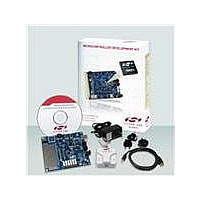
Manufacturer Part Number
C8051F800DK
Description
KIT DEV C8051F800
Manufacturer
Silicon Laboratories Inc
Type
MCUr
Specifications of C8051F800DK
Contents
Board, Cables, CD, Debugger, Power Supply
Processor To Be Evaluated
C8051F800
Data Bus Width
16 bit
Interface Type
USB
Operating Supply Voltage
7 V to 15 V
Lead Free Status / RoHS Status
Contains lead / RoHS non-compliant
For Use With/related Products
C8051F8xx
Lead Free Status / Rohs Status
Supplier Unconfirmed
Other names
336-1797


8.3.3. Settling Time Requirements
A minimum tracking time is required before each conversion to ensure that an accurate conversion is per-
formed. This tracking time is determined by any series impedance, including the AMUX0 resistance, the
the ADC0 sampling capacitance, and the accuracy required for the conversion. In delayed tracking mode,
three SAR clocks are used for tracking at the start of every conversion. For many applications, these three
SAR clocks will meet the minimum tracking time requirements.
Figure 8.3 shows the equivalent ADC0 input circuit. The required ADC0 settling time for a given settling
accuracy (SA) may be approximated by Equation 8.1. See Table 7.9 for ADC0 minimum settling time
requirements as well as the mux impedance and sampling capacitor values.
Where:
SA is the settling accuracy, given as a fraction of an LSB (for example, 0.25 to settle within 1/4 LSB)
t is the required settling time in seconds
R
n is the ADC resolution in bits (10).
TOTAL
is the sum of the AMUX0 resistance and any external source resistance.
Note: See electrical specification tables for R
Input Pin
Equation 8.1. ADC0 Settling Time Requirements
Figure 8.3. ADC0 Equivalent Input Circuits
t
=
RC
MUX Select
ln
Input
------ -
SA
= R
2
n
MUX
* C
Rev. 1.0
R
R
TOTAL
SAMPLE
MUX
C
SAMPLE
MUX
and C
C
SAMPLE
C8051F80x-83x
SAMPLE
parameters.
49
Related parts for C8051F800DK
Image
Part Number
Description
Manufacturer
Datasheet
Request
R

Part Number:
Description:
SMD/C°/SINGLE-ENDED OUTPUT SILICON OSCILLATOR
Manufacturer:
Silicon Laboratories Inc
Part Number:
Description:
Manufacturer:
Silicon Laboratories Inc
Datasheet:
Part Number:
Description:
N/A N/A/SI4010 AES KEYFOB DEMO WITH LCD RX
Manufacturer:
Silicon Laboratories Inc
Datasheet:
Part Number:
Description:
N/A N/A/SI4010 SIMPLIFIED KEY FOB DEMO WITH LED RX
Manufacturer:
Silicon Laboratories Inc
Datasheet:
Part Number:
Description:
N/A/-40 TO 85 OC/EZLINK MODULE; F930/4432 HIGH BAND (REV E/B1)
Manufacturer:
Silicon Laboratories Inc
Part Number:
Description:
EZLink Module; F930/4432 Low Band (rev e/B1)
Manufacturer:
Silicon Laboratories Inc
Part Number:
Description:
I°/4460 10 DBM RADIO TEST CARD 434 MHZ
Manufacturer:
Silicon Laboratories Inc
Part Number:
Description:
I°/4461 14 DBM RADIO TEST CARD 868 MHZ
Manufacturer:
Silicon Laboratories Inc
Part Number:
Description:
I°/4463 20 DBM RFSWITCH RADIO TEST CARD 460 MHZ
Manufacturer:
Silicon Laboratories Inc
Part Number:
Description:
I°/4463 20 DBM RADIO TEST CARD 868 MHZ
Manufacturer:
Silicon Laboratories Inc
Part Number:
Description:
I°/4463 27 DBM RADIO TEST CARD 868 MHZ
Manufacturer:
Silicon Laboratories Inc
Part Number:
Description:
I°/4463 SKYWORKS 30 DBM RADIO TEST CARD 915 MHZ
Manufacturer:
Silicon Laboratories Inc
Part Number:
Description:
N/A N/A/-40 TO 85 OC/4463 RFMD 30 DBM RADIO TEST CARD 915 MHZ
Manufacturer:
Silicon Laboratories Inc
Part Number:
Description:
I°/4463 20 DBM RADIO TEST CARD 169 MHZ
Manufacturer:
Silicon Laboratories Inc