C8051F800DK Silicon Laboratories Inc, C8051F800DK Datasheet - Page 5
C8051F800DK
Manufacturer Part Number
C8051F800DK
Description
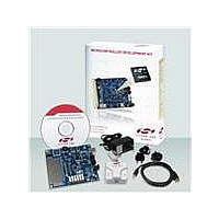
KIT DEV C8051F800
Manufacturer
Silicon Laboratories Inc
Type
MCUr
Specifications of C8051F800DK
Contents
Board, Cables, CD, Debugger, Power Supply
Processor To Be Evaluated
C8051F800
Data Bus Width
16 bit
Interface Type
USB
Operating Supply Voltage
7 V to 15 V
Lead Free Status / RoHS Status
Contains lead / RoHS non-compliant
For Use With/related Products
C8051F8xx
Lead Free Status / Rohs Status
Supplier Unconfirmed
Other names
336-1797


24. Cyclic Redundancy Check Unit (CRC0)............................................................. 159
25. Enhanced Serial Peripheral Interface (SPI0) ..................................................... 167
26. SMBus................................................................................................................... 180
23.1. Port I/O Modes of Operation.......................................................................... 139
23.2. Assigning Port I/O Pins to Analog and Digital Functions............................... 140
23.3. Priority Crossbar Decoder ............................................................................. 143
23.4. Port I/O Initialization ...................................................................................... 147
23.5. Port Match ..................................................................................................... 150
23.6. Special Function Registers for Accessing and Configuring Port I/O ............. 152
24.1. 16-bit CRC Algorithm..................................................................................... 160
24.2. 32-bit CRC Algorithm..................................................................................... 161
24.3. Preparing for a CRC Calculation ................................................................... 162
24.4. Performing a CRC Calculation ...................................................................... 162
24.5. Accessing the CRC0 Result .......................................................................... 162
24.6. CRC0 Bit Reverse Feature............................................................................ 166
25.1. Signal Descriptions........................................................................................ 168
25.2. SPI0 Master Mode Operation ........................................................................ 168
25.3. SPI0 Slave Mode Operation .......................................................................... 170
25.4. SPI0 Interrupt Sources .................................................................................. 171
25.5. Serial Clock Phase and Polarity .................................................................... 171
25.6. SPI Special Function Registers ..................................................................... 173
26.1. Supporting Documents .................................................................................. 181
26.2. SMBus Configuration..................................................................................... 181
26.3. SMBus Operation .......................................................................................... 181
26.4. Using the SMBus........................................................................................... 183
23.1.1. Port Pins Configured for Analog I/O...................................................... 139
23.1.2. Port Pins Configured For Digital I/O...................................................... 139
23.1.3. Interfacing Port I/O to 5 V Logic ............................................................ 140
23.2.1. Assigning Port I/O Pins to Analog Functions ........................................ 140
23.2.2. Assigning Port I/O Pins to Digital Functions.......................................... 141
23.2.3. Assigning Port I/O Pins to External Digital Event Capture Functions ... 142
25.1.1. Master Out, Slave In (MOSI)................................................................. 168
25.1.2. Master In, Slave Out (MISO)................................................................. 168
25.1.3. Serial Clock (SCK) ................................................................................ 168
25.1.4. Slave Select (NSS) ............................................................................... 168
26.3.1. Transmitter Vs. Receiver....................................................................... 182
26.3.2. Arbitration.............................................................................................. 182
26.3.3. Clock Low Extension............................................................................. 182
26.3.4. SCL Low Timeout.................................................................................. 182
26.3.5. SCL High (SMBus Free) Timeout ......................................................... 183
26.4.1. SMBus Configuration Register.............................................................. 183
26.4.2. SMB0CN Control Register .................................................................... 187
26.4.3. Hardware Slave Address Recognition .................................................. 189
26.4.2.1. Software ACK Generation ............................................................ 187
26.4.2.2. Hardware ACK Generation ........................................................... 187
Rev. 1.0
C8051F80x-83x
5
Related parts for C8051F800DK
Image
Part Number
Description
Manufacturer
Datasheet
Request
R

Part Number:
Description:
SMD/C°/SINGLE-ENDED OUTPUT SILICON OSCILLATOR
Manufacturer:
Silicon Laboratories Inc
Part Number:
Description:
Manufacturer:
Silicon Laboratories Inc
Datasheet:
Part Number:
Description:
N/A N/A/SI4010 AES KEYFOB DEMO WITH LCD RX
Manufacturer:
Silicon Laboratories Inc
Datasheet:
Part Number:
Description:
N/A N/A/SI4010 SIMPLIFIED KEY FOB DEMO WITH LED RX
Manufacturer:
Silicon Laboratories Inc
Datasheet:
Part Number:
Description:
N/A/-40 TO 85 OC/EZLINK MODULE; F930/4432 HIGH BAND (REV E/B1)
Manufacturer:
Silicon Laboratories Inc
Part Number:
Description:
EZLink Module; F930/4432 Low Band (rev e/B1)
Manufacturer:
Silicon Laboratories Inc
Part Number:
Description:
I°/4460 10 DBM RADIO TEST CARD 434 MHZ
Manufacturer:
Silicon Laboratories Inc
Part Number:
Description:
I°/4461 14 DBM RADIO TEST CARD 868 MHZ
Manufacturer:
Silicon Laboratories Inc
Part Number:
Description:
I°/4463 20 DBM RFSWITCH RADIO TEST CARD 460 MHZ
Manufacturer:
Silicon Laboratories Inc
Part Number:
Description:
I°/4463 20 DBM RADIO TEST CARD 868 MHZ
Manufacturer:
Silicon Laboratories Inc
Part Number:
Description:
I°/4463 27 DBM RADIO TEST CARD 868 MHZ
Manufacturer:
Silicon Laboratories Inc
Part Number:
Description:
I°/4463 SKYWORKS 30 DBM RADIO TEST CARD 915 MHZ
Manufacturer:
Silicon Laboratories Inc
Part Number:
Description:
N/A N/A/-40 TO 85 OC/4463 RFMD 30 DBM RADIO TEST CARD 915 MHZ
Manufacturer:
Silicon Laboratories Inc
Part Number:
Description:
I°/4463 20 DBM RADIO TEST CARD 169 MHZ
Manufacturer:
Silicon Laboratories Inc