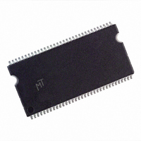
MT46V256M4TG-75:A Micron Technology Inc, MT46V256M4TG-75:A Datasheet - Page 37

MT46V256M4TG-75:A
Manufacturer Part Number
MT46V256M4TG-75:A
Description
IC DDR SDRAM 1GBIT 7.5NS 66TSOP
Manufacturer
Micron Technology Inc
Datasheet
1.MT46V256M4P-6TA_TR.pdf
(82 pages)
Specifications of MT46V256M4TG-75:A
Format - Memory
RAM
Memory Type
DDR SDRAM
Memory Size
1G (256M x 4)
Speed
7.5ns
Interface
Parallel
Voltage - Supply
2.3 V ~ 2.7 V
Operating Temperature
0°C ~ 70°C
Package / Case
66-TSOP
Lead Free Status / RoHS Status
Contains lead / RoHS non-compliant
Table 26:
PDF: 09005aef80a2f898/Source: 09005aef82a95a3a
DDR_x4x8x16_Core2.fm - 1Gb DDR: Rev. I, Core DDR: Rev. B 12/07 EN
From
Command
WRITE with auto
precharge
READ with auto
precharge
Command Delays
CL
RU
= CL rounded up to the next integer
WRITE or WRITE with auto precharge
WRITE or WRITE with auto precharge
READ or READ with auto precharge
READ or READ with auto precharge
3. Current state definitions:
4. AUTO REFRESH and LMR commands may only be issued when all banks are idle.
5. A BURST TERMINATE command cannot be issued to another bank; it applies to the bank
6. All states and sequences not shown are illegal or reserved.
7. READs or WRITEs listed in the “Command/Action” column include READs or WRITEs with
8. Requires appropriate DM masking.
9. A WRITE command may be applied after the completion of the READ burst; otherwise, a
that bank m is in such a state that the given command is allowable). Exceptions are covered
in the notes below.
represented by the current state only.
auto precharge enabled and READs or WRITEs with auto precharge disabled.
BURST TERMINATE must be used to end the READ burst prior to asserting a WRITE com-
mand.
• Idle: The bank has been precharged, and
• Row active: A row in the bank has been activated, and
• Read: A READ burst has been initiated, with auto precharge disabled, and has not yet
• Write: A WRITE burst has been initiated, with auto precharge disabled, and has not yet
• Read with auto precharge enabled: See note 3a below.
• Write with auto precharge enabled: See note 3a below.
bursts/accesses and no register accesses are in progress.
terminated or been terminated.
terminated or been terminated.
a. The read with auto precharge enabled or write with auto precharge enabled states
b. The minimum delay from a READ or WRITE command with auto precharge enabled,
To Command
can each be broken into two parts: the access period and the precharge period. For
read with auto precharge, the precharge period is defined as if the same burst was
executed with auto precharge disabled and then followed with the earliest possible
PRECHARGE command that still accesses all of the data in the burst. For write with
auto precharge, the precharge period begins when
if auto precharge was disabled. The access period starts with registration of the com-
mand and ends where the precharge period (or
concurrent auto precharge such that when a read with auto precharge is enabled or
a write with auto precharge is enabled, any command to other banks is allowed, as
long as that command does not interrupt the read or write data transfer already in
process. In either case, all other related limitations apply (for example, contention
between read data and write data must be avoided).
to a command to a different bank is summarized in Table 26.
PRECHARGE
PRECHARGE
ACTIVE
ACTIVE
37
Micron Technology, Inc., reserves the right to change products or specifications without notice.
t
RP has been met.
with Concurrent Auto Precharge
1Gb: x4, x8, x16 DDR SDRAM
[1 + (BL/2)] ×
t
RP) begins. This device supports
[CL
Minimum Delay
t
WR ends, with
RU
t
RCD has been met. No data
(BL/2) ×
(BL/2) ×
+
1
1
1
1
(BL/2)] ×
©2003 Micron Technology, Inc. All rights reserved.
t
t
t
t
CK
CK
CK
CK
t
CK +
t
t
CK
CK
t
t
CK
WTR
t
WR measured as
Commands


