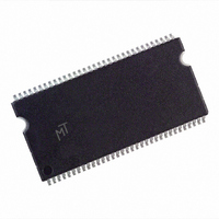
MT46V256M4TG-75:A Micron Technology Inc, MT46V256M4TG-75:A Datasheet - Page 12

MT46V256M4TG-75:A
Manufacturer Part Number
MT46V256M4TG-75:A
Description
IC DDR SDRAM 1GBIT 7.5NS 66TSOP
Manufacturer
Micron Technology Inc
Datasheet
1.MT46V256M4P-6TA_TR.pdf
(82 pages)
Specifications of MT46V256M4TG-75:A
Format - Memory
RAM
Memory Type
DDR SDRAM
Memory Size
1G (256M x 4)
Speed
7.5ns
Interface
Parallel
Voltage - Supply
2.3 V ~ 2.7 V
Operating Temperature
0°C ~ 70°C
Package / Case
66-TSOP
Lead Free Status / RoHS Status
Contains lead / RoHS non-compliant
Electrical Specifications – I
Table 5:
PDF: 09005aef80a2f898/Source: 09005aef82a95a3a
1Gb_DDR_x4x8x16_D2.fm - 1Gb DDR: Rev. I, Core DDR: Rev. B 12/07 EN
Parameter/Condition
Operating one-bank active-precharge current:
t
changing once per clock cycle; Address and control inputs
changing once every two clock cycles
Operating one-bank active-read-precharge current:
BL = 4;
Address and control inputs changing once per clock cycle
Precharge power-down standby current: All banks
idle; Power-down mode;
Idle standby current: CS# = HIGH; All banks are idle;
t
inputs changing once per clock cycle. V
DQS, and DM
Active power-down standby current: One bank active;
Power-down mode;
Active standby current: CS# = HIGH; CKE = HIGH; One
bank active;
and DQS inputs changing twice per clock cycle; Address
and other control inputs changing once per clock cycle
Operating burst read current: BL = 2;
reads; One bank active; Address and control inputs changing
once per clock cycle;
Operating burst write current: BL = 2; Continuous
burst writes; One bank active; Address and control inputs
changing once per clock cycle;
and DQS inputs changing twice per clock cycle
Auto refresh burst current:
Self refresh current: CKE ≤ 0.2V
Operating bank interleave read current: Four bank
interleaving READs (BL = 4) with auto precharge;
t
change only during ACTIVE, READ, or WRITE commands
RC =
CK =
RC = MIN;
t
t
RC (MIN);
CK (MIN); CKE = HIGH; Address and other control
t
RC =
t
CK =
t
I
Notes 1–5, 11, 13, 15, 47 apply to the entire table; Notes appear on page 26–31; See also Table 7 on page 14;
V
0°C ≤ T
t
RC =
DD
RC (MIN);
DD
t
Q = +2.6V ±0.1V, V
Specifications and Conditions (x4, x8)
CK =
t
CK (MIN); Address and control inputs
t
RAS (MAX);
A
t
t
CK =
CK =
≤ +70°C
t
CK (MIN); DQ, DM, and DQS inputs
t
CK =
t
t
CK =
CK (MIN);
t
CK (MIN); CKE = LOW
t
CK (MIN); I
t
t
t
CK =
CK (MIN); CKE = LOW
CK =
DD
I
OUT
t
= +2.6V ±0.1V (-5B); V
t
CK (MIN); DQ, DM,
CK (MIN); DQ, DM,
IN
t
t
Standard
= 0mA
REFC =
REFC = 7.8µs
Continuous burst
OUT
= V
DD
REF
= 0mA;
t
for DQ,
RFC (MIN)
12
DD
Q = +2.5V ±0.2V, V
Symbol
I
I
I
I
I
I
I
DD
DD
DD
DD
I
I
DD
DD
DD
I
I
I
DD
DD
DD
DD
DD
4W
3N
5A
2P
3P
4R
2F
0
1
5
6
7
Micron Technology, Inc., reserves the right to change products or specifications without notice.
165
200
225
235
345
530
-5B
13
70
40
55
13
10
Electrical Specifications – I
DD
1Gb: x4, x8, x16 DDR SDRAM
= +2.5V ±0.2V (-6T, -75);
160
195
220
230
340
525
-6T
10
65
35
50
10
9
©2003 Micron Technology, Inc. All rights reserved.
-75
145
180
200
210
330
485
10
60
30
45
10
9
Units
mA
mA
mA
mA
mA
mA
mA
mA
mA
mA
mA
mA
Notes
23, 48
23, 48
23, 49
24, 33
24, 33
23, 48
28, 50
51
23
23
50
12
DD


