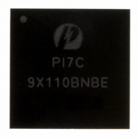
PI7C9X110BNBE Pericom Semiconductor, PI7C9X110BNBE Datasheet - Page 90

PI7C9X110BNBE
Manufacturer Part Number
PI7C9X110BNBE
Description
IC PCIE TO PCI REV BRG 160LFBGA
Manufacturer
Pericom Semiconductor
Specifications of PI7C9X110BNBE
Applications
PCI-to-PCI Bridge
Interface
I²C
Voltage - Supply
1.8 V
Package / Case
160-LBGA
Mounting Type
Surface Mount
Operating Temperature (min)
-40C
Operating Temperature Classification
Industrial
Operating Temperature (max)
85C
Rad Hardened
No
Maximum Operating Temperature
+ 85 C
Minimum Operating Temperature
- 40 C
Mounting Style
SMD/SMT
Lead Free Status / RoHS Status
Lead free / RoHS Compliant
Lead Free Status / RoHS Status
Lead free / RoHS Compliant, Compliant
Available stocks
Company
Part Number
Manufacturer
Quantity
Price
Company:
Part Number:
PI7C9X110BNBE
Manufacturer:
PLX
Quantity:
1 238
Company:
Part Number:
PI7C9X110BNBE
Manufacturer:
PERICOM31
Quantity:
193
Part Number:
PI7C9X110BNBE
Manufacturer:
PERICOM
Quantity:
20 000
7.5.39 UPSTREAM MEMORY 3 BASE ADDRESS REGISTER – OFFSET 60h
Pericom Semiconductor – Confidential
BIT
2:1
3
13:4
31:14
BIT
0
2:1
3
11:4
31:12
FUNCTION
Address Type
Prefetchable control
Reserved
Base Address
FUNCTION
Space Indicator
Address Type
Prefetchable control
Reserved
Base Address
RW/RO
RW/RO
TYPE
TYPE
RO
RO
RO
RO
RO
RO
RO
Page 90 of 144
DESCRIPTION
00: 32-bit address decode range
01, 10 and 11: reserved
Reset to 00
0: Memory space is non-prefetchable
1: Memory space is prefetchable
Reset to 0
Reset to 0
This Base Address register defines the address range for upstream memory
transactions. PI7C9X110 uses a lookup table to do the address translation.
The address range of this register is from 16KB to 2GB in memory space.
The address range is divided into 64 pages. The size of each page is defined
by Memory Address Forwarding Control register (Offset 6Ah), which is
initialized by EEPROM (I2C) or SM Bus or local processor. Writing a zero
to the bit [0] of the look up table entry can disable the corresponding page of
this register (CSR Offset 1FFh: 100h).
The number of writeable bit may change depending on the page size setup.
Reset to 00000h
DESCRIPTION
0: Memory space
1: IO space
Reset to 0
00: 32-bit address decode range
01: 64-bit address decode range
10 and 11: reserved
Reset to 00
0: Memory space is non-prefetchable
1: Memory space is prefetchable
Reset to 0
Reset to 0
The size and type of this Base Address Register are defined from Upstream
Memory 3 Setup Register (CSR Offset 034h), which can be initialized by
EEPROM (I2C) or SM Bus or Local Processor. Writing a zero to bit [31] of
the setup registers (CSR Offset 034h and 038h) to disable this register. The
range of this register is from 4KB to 9EB for memory space. PI7C9X110
uses this register and the Upstream Memory 3 Upper Base Address Register
when 64-bit addressing programmed (bit [21] of Offset 68h). When 64-bit
addressing is disabled, no address translation is performed. All 64-bit
address transactions on the secondary interface falling outside of the
Downstream Memory 3 address range are forwarded upstream.
Reset to 00000h
April 2010, Revision 3.0
PCIe-to-PCI Reversible Bridge
PI7C9X110


