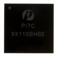
PI7C9X110BNBE Pericom Semiconductor, PI7C9X110BNBE Datasheet - Page 135

PI7C9X110BNBE
Manufacturer Part Number
PI7C9X110BNBE
Description
IC PCIE TO PCI REV BRG 160LFBGA
Manufacturer
Pericom Semiconductor
Specifications of PI7C9X110BNBE
Applications
PCI-to-PCI Bridge
Interface
I²C
Voltage - Supply
1.8 V
Package / Case
160-LBGA
Mounting Type
Surface Mount
Operating Temperature (min)
-40C
Operating Temperature Classification
Industrial
Operating Temperature (max)
85C
Rad Hardened
No
Maximum Operating Temperature
+ 85 C
Minimum Operating Temperature
- 40 C
Mounting Style
SMD/SMT
Lead Free Status / RoHS Status
Lead free / RoHS Compliant
Lead Free Status / RoHS Status
Lead free / RoHS Compliant, Compliant
Available stocks
Company
Part Number
Manufacturer
Quantity
Price
Company:
Part Number:
PI7C9X110BNBE
Manufacturer:
PLX
Quantity:
1 238
Company:
Part Number:
PI7C9X110BNBE
Manufacturer:
PERICOM31
Quantity:
193
Part Number:
PI7C9X110BNBE
Manufacturer:
PERICOM
Quantity:
20 000
14.2 BYPASS REGISTER
14.3 DEVICE ID REGISTER
14.4 BOUNDARY SCAN REGISTER
14.5 JTAG BOUNDARY SCAN REGISTER ORDER
PI7C9X110 implements a 5-bit Instruction register to control the operation of the JTAG logic. The defined
instruction codes are shown in Table 14-1. Those bit combinations that are not listed are equivalent to the BYPASS
(11111) instruction:
Table 14-1 Instruction register codes
The required bypass register (one-bit shift register) provides the shortest path between TDI and TDO when a bypass
instruction is in effect. This allows rapid movement of test data to and from other components on the board. This
path can be selected when no test operation is being performed on the PI7C9X110.
This register identifies Pericom as the manufacturer of the device and details the part number and revision number
for the device.
Table 14-2 JTAG device ID register
The boundary scan register has a set of serial shift-register cells. A chain of boundary scan cells is formed by
connected the internal signal of the PI7C9X110 package pins. The VDD, VSS, and JTAG pins are not in the
boundary scan chain. The input to the shift register is TDI and the output from the shift register is TDO. There are 4
different types of boundary scan cells, based on the function of each signal pin.
The boundary scan register cells are dedicated logic and do not have any system function. Data may be loaded into
the boundary scan register master cells from the device input pins and output pin-drivers in parallel by the
mandatory SAMPLE and EXTEST instructions. Parallel loading takes place on the rising edge of TCK.
Pericom Semiconductor – Confidential
Table 14-3 JTAG boundary scar register definition
Instruction
EXTEST
SAMPLE
HIGHZ
CLAMP
IDCODE
BYPASS
INT_SCAN
MEM_BIST
Bit
31:28
27:12
11:1
0
Operation Code (binary)
Type
RO
RO
RO
RO
00000
00001
00101
00100
01100
11111
00010
01010
Register Selected
Boundary Scan
Boundary Scan
Bypass
Bypass
Device ID
Bypass
Internal Scan
Memory BIST
Value
01h
E110h
23Fh
1b
Page 135 of 144
Operation
Drives / receives off-chip test data
Samples inputs / pre-loads outputs
Tri-states output and I/O pins except TDO pin
Drives pins from boundary-scan register and selects Bypass register
for shifts
Accesses the Device ID register, to read manufacturer ID, part
number, and version number
Selected Bypass Register
Scan test
Memory BIST test
Description
Version number
Last 4 digits (hex) of the die part number
Pericom identifier assigned by JEDEC
Fixed bit equal to 1’b1
April 2010, Revision 3.0
PCIe-to-PCI Reversible Bridge
PI7C9X110


