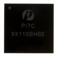
PI7C9X110BNBE Pericom Semiconductor, PI7C9X110BNBE Datasheet - Page 122

PI7C9X110BNBE
Manufacturer Part Number
PI7C9X110BNBE
Description
IC PCIE TO PCI REV BRG 160LFBGA
Manufacturer
Pericom Semiconductor
Specifications of PI7C9X110BNBE
Applications
PCI-to-PCI Bridge
Interface
I²C
Voltage - Supply
1.8 V
Package / Case
160-LBGA
Mounting Type
Surface Mount
Operating Temperature (min)
-40C
Operating Temperature Classification
Industrial
Operating Temperature (max)
85C
Rad Hardened
No
Maximum Operating Temperature
+ 85 C
Minimum Operating Temperature
- 40 C
Mounting Style
SMD/SMT
Lead Free Status / RoHS Status
Lead free / RoHS Compliant
Lead Free Status / RoHS Status
Lead free / RoHS Compliant, Compliant
Available stocks
Company
Part Number
Manufacturer
Quantity
Price
Company:
Part Number:
PI7C9X110BNBE
Manufacturer:
PLX
Quantity:
1 238
Company:
Part Number:
PI7C9X110BNBE
Manufacturer:
PERICOM31
Quantity:
193
Part Number:
PI7C9X110BNBE
Manufacturer:
PERICOM
Quantity:
20 000
7.6
7.6.1
7.6.2
7.6.3
7.6.4
Control and Status Registers (CSR’s) can be accessed by Memory or I/O transactions from both primary and
secondary ports. The CSR’s are defined and to be used along with configuration registers (see previous section 7.5
for details) for non-transparent bridge operations.
Pericom Semiconductor – Confidential
CONTROL AND STATUS REGISTERS FOR NON-TRANSPARENT BRIDGE
MODE
RESERVED REGISTERS – OFFSET 000h TO 004h
DOWNSTREAM MEMORY 2 TRANSLATED BASE REGISTER – OFFSET 008h
DOWNSTREAM MEMORY 2 SETUP REGISTER – OFFSET 00Ch
DOWNSTREAM MEMORY 3 TRANSLATED BASE REGISTER – OFFSET 010h
Register Type
RO
ROS
RW
RWC
RWS
RWCS
BIT
11:0
31:12
BIT
0
2:1
3
11:4
30:12
31
BIT
11:0
FUNCTION
Reserved
Downstream Memory 2
Translated Base
FUNCTION
Type Selector
Address Type
Prefetchable Control
Reserved
Base Address Register Size
Base Address Register
Enable
FUNCTION
Reserved
TYPE
TYPE
TYPE
(WS)
(WS)
(WS)
(WS)
RW
RO
RO
RO
RO
RO
RO
RO
RO
Page 122 of 144
Descriptions
Read Only
Read Only and Sticky
Read/Write
Read/Write “1” to clear
Read/Write and Sticky
Read/Write “1” to clear and Sticky
DESCRIPTION
Reset to 000h
Define the translated base address for downstream memory transactions
whose initiator addresses fall into Downstream Memory 2 address range. The
number of bits that are used for translated base is determined by its setup
register (offset 00Ch)
Reset to 00000h
DESCRIPTION
0: Memory space is requested
Reset to 0
00: 32-bit address space
01: 64-bit address space
Reset to 00
0: Non-prefetchable
1: Prefetchable
Reset to 0
Reset to 00
0: Set the corresponding bit in the Base Address Register to read only
1: Set the corresponding bit in the Base Address Register to read/write in
order to control the size of the address range
Reset to 00000h
0: Disable this Base Address Register
1: Enable this Base Address Register
Reset to 0
DESCRIPTION
Reset to 000000
April 2010, Revision 3.0
PCIe-to-PCI Reversible Bridge
PI7C9X110


