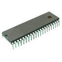
ST72C334N2B6 STMicroelectronics, ST72C334N2B6 Datasheet - Page 66

ST72C334N2B6
Manufacturer Part Number
ST72C334N2B6
Description
Microcontrollers (MCU) Flash 8K SPI/SCI
Manufacturer
STMicroelectronics
Datasheet
1.ST72C334N2T6.pdf
(126 pages)
Specifications of ST72C334N2B6
Data Bus Width
8 bit
Program Memory Type
Flash
Program Memory Size
8 KB
Data Ram Size
384 B
Interface Type
SCI, SPI
Maximum Clock Frequency
8 MHz
Number Of Programmable I/os
44
Number Of Timers
16 bit
Operating Supply Voltage
3.2 V to 5.5 V
Maximum Operating Temperature
+ 85 C
Mounting Style
Through Hole
Package / Case
SDIP-56
Minimum Operating Temperature
- 40 C
On-chip Adc
8 bit
Lead Free Status / Rohs Status
No
Available stocks
Company
Part Number
Manufacturer
Quantity
Price
Company:
Part Number:
ST72C334N2B6
Manufacturer:
ST
Quantity:
365
ST72334J/N, ST72314J/N, ST72124J
16-BIT TIMER (Cont’d)
CONTROL REGISTER 2 (CR2)
Read/Write
Reset Value: 0000 0000 (00h)
Bit 7 = OC1E Output Compare 1 Pin Enable.
This bit is used only to output the signal from the
timer on the OCMP1 pin (OLV1 in Output Com-
pare mode, both OLV1 and OLV2 in PWM and
one-pulse mode). Whatever the value of the OC1E
bit, the Output Compare 1 function of the timer re-
mains active.
0: OCMP1 pin alternate function disabled (I/O pin
1: OCMP1 pin alternate function enabled.
Bit 6 = OC2E Output Compare 2 Enable.
This bit is used only to output the signal from the
timer on the OCMP2 pin (OLV2 in Output Com-
pare mode). Whatever the value of the OC2E bit,
the Output Compare 2 function of the timer re-
mains active.
0: OCMP2 pin alternate function disabled (I/O pin
1: OCMP2 pin alternate function enabled.
Bit 5 = OPM One Pulse Mode.
0: One Pulse Mode is not active.
1: One Pulse Mode is active, the ICAP1 pin can be
66/125
OC1E OC2E OPM PWM CC1 CC0 IEDG2 EXEDG
free for general-purpose I/O).
free for general-purpose I/O).
used to trigger one pulse on the OCMP1 pin; the
active transition is given by the IEDG1 bit. The
length of the generated pulse depends on the
contents of the OC1R register.
7
0
Bit 4 = PWM Pulse Width Modulation.
0: PWM mode is not active.
1: PWM mode is active, the OCMP1 pin outputs a
Bit 3, 2 = CC1-CC0 Clock Control.
The value of the timer clock depends on these bits:
Table 14. Clock Control Bits
Bit 1 = IEDG2 Input Edge 2.
This bit determines which type of level transition
on the ICAP2 pin will trigger the capture.
0: A falling edge triggers the capture.
1: A rising edge triggers the capture.
Bit 0 = EXEDG External Clock Edge.
This bit determines which type of level transition
on the external clock pin EXTCLK will trigger the
free running counter.
0: A falling edge triggers the free running counter.
1: A rising edge triggers the free running counter.
External Clock (where
programmable cyclic signal; the length of the
pulse depends on the value of OC1R register;
the period depends on the value of OC2R regis-
ter.
Timer Clock
available)
f
f
f
CPU
CPU
CPU
/ 4
/ 2
/ 8
CC1
0
0
1
1
CC0
0
1
0
1


