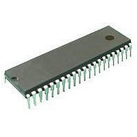
ST72C334N2B6 STMicroelectronics, ST72C334N2B6 Datasheet - Page 121

ST72C334N2B6
Manufacturer Part Number
ST72C334N2B6
Description
Microcontrollers (MCU) Flash 8K SPI/SCI
Manufacturer
STMicroelectronics
Datasheet
1.ST72C334N2T6.pdf
(126 pages)
Specifications of ST72C334N2B6
Data Bus Width
8 bit
Program Memory Type
Flash
Program Memory Size
8 KB
Data Ram Size
384 B
Interface Type
SCI, SPI
Maximum Clock Frequency
8 MHz
Number Of Programmable I/os
44
Number Of Timers
16 bit
Operating Supply Voltage
3.2 V to 5.5 V
Maximum Operating Temperature
+ 85 C
Mounting Style
Through Hole
Package / Case
SDIP-56
Minimum Operating Temperature
- 40 C
On-chip Adc
8 bit
Lead Free Status / Rohs Status
No
Available stocks
Company
Part Number
Manufacturer
Quantity
Price
Company:
Part Number:
ST72C334N2B6
Manufacturer:
ST
Quantity:
365
9.2 DEVICE CONFIGURATION AND ORDERING
INFORMATION
Each device is available for production in user pro-
grammable versions (FLASH) as well as in factory
coded versions (ROM).
FLASH devices are shipped to customers with a
default content (FFh), while ROM factory coded
parts contain the code supplied by the customer.
This implies that FLASH devices have to be con-
figured by the customer using the Option Bytes
while the ROM devices are factory-configured.
9.2.1 Option Bytes
The two Option Bytes allow the hardware configu-
ration of the microcontroller to be selected.
The Option Bytes have no address in the memory
map and can be accessed only in programming
mode (for example using a standard ST7
4programming tool). The default contents of the
FLASH is fixed to FFh. This means that all the op-
tions have “1” as their default value.
In masked ROM devices, the Option Bytes are
fixed in hardware by the ROM code.
USER OPTION BYTE 1
Bit 7:2 = Reserved, must always be 1.
Bit 1 = 56/42 Package configuration .
This option bit allows to configure the device ac-
cording to the package.
0: 42 and 44 pin.
1: 56 and 64 pin.
Bit 0 = FMP Full memory protection.
This option bit enables or disables external access
to the internal program memory (read-out protec-
tion). Clearing this bit causes the erasing (to 00h)
of the whole memory (including the option byte).
0: Program memory not read-out protected
1: Program memory read-out protected
7
1
1
1
1
1
1
56/42 FMP
0
USER OPTION BYTE 2
Bit 7 = CFC Clock filter control on/off
This option bit enables or disables the clock filter
(CF) features.
0: Clock filter enabled
1: Clock filter disabled
Bit 6:4 = OSC[2:0] Oscillator selection
These three option bits can be used to select the
main oscillator as shown in Table 24.
Table 24. Main Oscillator Configuration
Bit 3:2 = LVD[1:0] Low voltage detection selection
These option bits enable the LVD block with a se-
lected threshold as shown in Table 25.
Table 25. LVD Threshold Configuration
Bit 1 = WDG HALT Watchdog and halt mode
This option bit determines if a RESET is generated
when entering HALT mode while the Watchdog is
active.
0: No Reset generation when entering Halt mode
1: Reset generation when entering Halt mode
Bit 0 = WDG SW Hardware or software watchdog
This option bit selects the watchdog type.
0: Hardware (watchdog always enabled)
1: Software (watchdog to be enabled by software)
Medium-high Speed Resonator
Medium Voltage Threshold (f
CFC OSC2 OSC1 OSC0 LVD1 LVD0
Medium-low Speed Resonator
Lowest Voltage Threshold (f
7
External Clock (Stand-by)
Highest Voltage Threshold (V
High Speed Resonator
Low Speed Resonator
Selected Oscillator
ST72334J/N, ST72314J/N, ST72124J
External RC
Internal RC
Configuratio n
LVD Off
OSC
OSC
DD
OSC2 OSC1 OSC0
16MHz)
8MHz)
~5V)
1
1
1
1
0
0
0
0
HALT
WDG
LVD1 LVD0
1
1
0
0
1
1
0
0
1
1
0
0
121/125
WDG
SW
1
0
1
0
1
0
1
0
1
0
1
0
0


