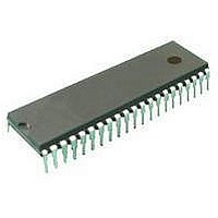
ST72C334N2B6 STMicroelectronics, ST72C334N2B6 Datasheet - Page 116

ST72C334N2B6
Manufacturer Part Number
ST72C334N2B6
Description
Microcontrollers (MCU) Flash 8K SPI/SCI
Manufacturer
STMicroelectronics
Datasheet
1.ST72C334N2T6.pdf
(126 pages)
Specifications of ST72C334N2B6
Data Bus Width
8 bit
Program Memory Type
Flash
Program Memory Size
8 KB
Data Ram Size
384 B
Interface Type
SCI, SPI
Maximum Clock Frequency
8 MHz
Number Of Programmable I/os
44
Number Of Timers
16 bit
Operating Supply Voltage
3.2 V to 5.5 V
Maximum Operating Temperature
+ 85 C
Mounting Style
Through Hole
Package / Case
SDIP-56
Minimum Operating Temperature
- 40 C
On-chip Adc
8 bit
Lead Free Status / Rohs Status
No
Available stocks
Company
Part Number
Manufacturer
Quantity
Price
Company:
Part Number:
ST72C334N2B6
Manufacturer:
ST
Quantity:
365
ST72334J/N, ST72314J/N, ST72124J
MEMORY AND PERIPHERAL CHARACTERISTICS (Cont’d)
Notes:
1) Unless otherwise specified, typical data are based on T
lines and are not tested.
2) Data based on characterization results, not tested in production.
3) Tested in production at T
4) ADC Accuracy vs. Negative Injection Current:
For I
for each 10K
under worst-case conditions for injection:
- negative injection
- injection to an Input with analog capability, adjacent to the enabled Analog Input
- at 5V V
116/125
ADC Analog to Digital Converter (8-bit)
Symbol
f
|TUE|
OE
GE
|DLE|
|ILE|
V
I
t
t
t
R
R
C
ADC
ADC
STAB
LOAD
CONV
255
254
253
AIN
AIN
ADC
SAMPLE
7
6
5
4
3
2
1
INJ-
0
V
SSA
=0.8mA, the typical leakage induced inside the die is 1.6 A and the effect on the ADC accuracy is a loss of 1 LSB
Digital Result ADCDR
DD
1
Analog control frequency
Total unadjusted error
Offset error
Gain Error
Differential linearity error
Integral linearity error
Conversion range voltage
A/D conversion supply current
Stabilization time after ADC enable
Sample capacitor loading time
Hold conversion time
External input resistor
Internal input resistor
Sample capacitor
supply, and worst case temperature.
OE
1LS B
increase of the external analog source impedance. This effect on the ADC accuracy has been observed
2
i deal
3
TUE
4)
=
4)
Parameter
V
---------------------------------------- -
4
D D A
A
=25 C, characterized over the whole temperature range.
256
5
1 LSB (ideal)
–
V
4)
S SA
4)
6
4)
ILE
7
(2)
DLE
T
V
f
V
CPU
A
f
DD
DD
CPU
=25 C,V
253 254 255 256
(3)
=8MHz, f
=V
=V
=8MHz,f
DDA
DDA
Conditions
A
=25 C and V
(1)
DD
=5V
=5V
GE
ADC
=V
ADC
V
DDA
=4MHz
=4MHz
DDA
=5V,
DD
-V
(1) Example of an actual transfer curve
(2) The ideal transfer curve
(3) End point correlation line
TUE=Total Unadjusted Error: maximum deviation
between the actual and the ideal transfer curves.
OE=Offset Error: deviation between the first actual
transition and the first ideal one.
GE=Gain Error: deviation between the last ideal
transition and the last actual one.
DLE=Differential Linearity Error: maximum devia-
tion between actual steps and the ideal one.
ILE=Integral Linearity Error: maximum deviation
between any actual transition and the end point
correlation line.
3)
SS
V
in
=5V. They are given only as design guide-
(LSB
V
Min
-0.5
-0.5
SSA
ideal
)
Typ
1.5
1
6
1
4
2
8
1)
V
15
Max
4
0.5
0.5
0.5
0.5
DDA
1
1
2)
2)
1/f
1/f
Unit
MHz
LSB
mA
k
k
pF
V
ADC
ADC
s
s
s


