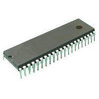
ST72C334N2B6 STMicroelectronics, ST72C334N2B6 Datasheet - Page 61

ST72C334N2B6
Manufacturer Part Number
ST72C334N2B6
Description
Microcontrollers (MCU) Flash 8K SPI/SCI
Manufacturer
STMicroelectronics
Datasheet
1.ST72C334N2T6.pdf
(126 pages)
Specifications of ST72C334N2B6
Data Bus Width
8 bit
Program Memory Type
Flash
Program Memory Size
8 KB
Data Ram Size
384 B
Interface Type
SCI, SPI
Maximum Clock Frequency
8 MHz
Number Of Programmable I/os
44
Number Of Timers
16 bit
Operating Supply Voltage
3.2 V to 5.5 V
Maximum Operating Temperature
+ 85 C
Mounting Style
Through Hole
Package / Case
SDIP-56
Minimum Operating Temperature
- 40 C
On-chip Adc
8 bit
Lead Free Status / Rohs Status
No
Available stocks
Company
Part Number
Manufacturer
Quantity
Price
Company:
Part Number:
ST72C334N2B6
Manufacturer:
ST
Quantity:
365
16-BIT TIMER (Cont’d)
6.4.3.5 Forced Compare
In this section i may represent 1 or 2.
The following bits of the CR1 register are used:
When the FOLV i bit is set by software, the OLVL i
bit is copied to the OCMP i pin. The OLV i bit has to
be toggled in order to toggle the OCMP i pin when
it is enabled (OC i E bit=1). The OCF i bit is then not
set by hardware, and thus no interrupt request is
generated.
FOLVL i bits have no effect in both one pulse mode
and PWM mode.
6.4.3.6 One Pulse Mode
One Pulse mode enables the generation of a
pulse when an external event occurs. This mode is
selected via the OPM bit in the CR2 register.
The one pulse mode uses the Input Capture1
function and the Output Compare1 function.
Procedure:
To use one pulse mode:
1. Load the OC1R register with the value corre-
2. Select the following in the CR1 register:
3. Select the following in the CR2 register:
sponding to the length of the pulse (see the for-
mula in Section 6.4.3.7).
– Using the OLVL1 bit, select the level to be ap-
– Using the OLVL2 bit, select the level to be ap-
– Select the edge of the active transition on the
– Set the OC1E bit, the OCMP1 pin is then ded-
– Set the OPM bit.
– Select the timer clock CC1-CC0 (see Table 14
plied to the OCMP1 pin after the pulse.
plied to the OCMP1 pin during the pulse.
ICAP1 pin with the IEDG1 bit (the ICAP1 pin
must be configured as floating input).
icated to the Output Compare 1 function.
Clock Control Bits).
FOLV2 FOLV1 OLVL2
OLVL1
Then, on a valid event on the ICAP1 pin, the coun-
ter is initialized to FFFCh and OLVL2 bit is loaded
on the OCMP1 pin, the ICF1 bit is set and the val-
ue FFFDh is loaded in the IC1R register.
When the value of the counter is equal to the value
of the contents of the OC1R register, the OLVL1
bit is output on the OCMP1 pin, (See Figure 44).
Notes:
1. The OCF1 bit cannot be set by hardware in one
2. The ICF1 bit is set when an active edge occurs
3. When the Pulse Width Modulation (PWM) and
4. If OLVL1=OLVL2 a continuous signal will be
5. The ICAP1 pin can not be used to perform input
6. When the one pulse mode is used OC1R is
pulse mode but the OCF2 bit can generate an
Output Compare interrupt.
and can generate an interrupt if the ICIE bit is
set.
One Pulse Mode (OPM) bits are both set, the
PWM mode is the only active one.
seen on the OCMP1 pin.
capture. The ICAP2 pin can be used to perform
input capture (ICF2 can be set and IC2R can be
loaded) but the user must take care that the
counter is reset each time a valid edge occurs
on the ICAP1 pin and ICF1 can also generates
interrupt if ICIE is set.
dedicated to this mode. Nevertheless OC2R
and OCF2 can be used to indicate a period of
time has been elapsed but cannot generate an
output waveform because the level OLVL2 is
dedicated to the one pulse mode.
event occurs
ST72334J/N, ST72314J/N, ST72124J
on ICAP1
Counter
= OC1R
When
When
One pulse mode cycle
OCMP1 = OLVL2
OCMP1 = OLVL1
Counter is reset
ICF1 bit is set
to FFFCh
61/125


