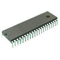
ST72C334N2B6 STMicroelectronics, ST72C334N2B6 Datasheet - Page 42

ST72C334N2B6
Manufacturer Part Number
ST72C334N2B6
Description
Microcontrollers (MCU) Flash 8K SPI/SCI
Manufacturer
STMicroelectronics
Datasheet
1.ST72C334N2T6.pdf
(126 pages)
Specifications of ST72C334N2B6
Data Bus Width
8 bit
Program Memory Type
Flash
Program Memory Size
8 KB
Data Ram Size
384 B
Interface Type
SCI, SPI
Maximum Clock Frequency
8 MHz
Number Of Programmable I/os
44
Number Of Timers
16 bit
Operating Supply Voltage
3.2 V to 5.5 V
Maximum Operating Temperature
+ 85 C
Mounting Style
Through Hole
Package / Case
SDIP-56
Minimum Operating Temperature
- 40 C
On-chip Adc
8 bit
Lead Free Status / Rohs Status
No
Available stocks
Company
Part Number
Manufacturer
Quantity
Price
Company:
Part Number:
ST72C334N2B6
Manufacturer:
ST
Quantity:
365
ST72334J/N, ST72314J/N, ST72124J
6 ON-CHIP PERIPHERALS
6.1 I/O PORTS
6.1.1 Introduction
The I/O ports offer different functional modes:
– transfer of data through digital inputs and outputs
and for specific pins:
– external interrupt generation
– alternate signal input/output for the on-chip pe-
An I/O port contains up to 8 pins. Each pin can be
programmed independently as digital input (with or
without interrupt generation) or digital output.
6.1.2 Functional Description
Each port is associated to 2 main registers:
– Data Register (DR)
– Data Direction Register (DDR)
and one optional register:
– Option Register (OR)
Each I/O pin may be programmed using the corre-
sponding register bits in DDR and OR registers: bit
X corresponding to pin X of the port. The same cor-
respondence is used for the DR register.
The following description takes into account the
OR register, for specific port which do not provide
this register refer to the I/O Port Implementation
section. The generic I/O block diagram is shown
on Figure 32
Input Modes
The input configuration is selected by clearing the
corresponding DDR register bit.
In this case, reading the DR register returns the
digital value applied to the external I/O pin.
Different input modes can be selected by software
through the OR register.
Note1: Writing the DR register modifies the latch
value but does not affect the pin status.
Note2: When switching from input to output mode,
the DR register has to be written first to drive the
correct level on the pin as soon as the ports is con-
figured as an output.
External interrupt function
When an I/O is configured in Input with Interrupt,
an event on this I/O can generate an external In-
terrupt request to the CPU.
Each pin can independently generate an Interrupt
request. The interrupt sensitivity is given inde-
pendently according to the description mentioned
in the Miscellaneous register.
42/125
ripherals (SPI, SCI, TIMERs...).
Each external interrupt vector is linked to a dedi-
cated group of I/O port pins (see Interrupt section).
If more than one input pins are selected simultane-
ously as interrupt source, these are logically AND-
ed. For this reason if one of the interrupt pins is
tied low, it masks the other ones.
In case of a floating input with interrupt configura-
tion, special cares mentioned in the I/O port imple-
mentation section have to be taken.
Output Mode
The output configuration is selected by setting the
corresponding DDR register bit.
In this case, writing the DR register applies this
digital value to the I/O pin through the latch. Then
reading the DR register returns the previously
stored value.
Two different output modes can be selected by
software through the OR register: Output push-pull
and open-drain.
DR register value and output pin status:
Note: In this mode, interrupt function is disabled.
Alternate function
When an on-chip peripheral is configured to use a
pin, the alternate function is automatically select-
ed. This alternate function takes priority over the
standard I/O programming.
When the signal is coming from an on-chip periph-
eral, the I/O pin is automatically configured in out-
put mode (push-pull or open drain according to the
peripheral).
When the signal is going to an on-chip peripheral,
the I/O pin has to be configured in input mode. In
this case, the pin’s state is also digitally readable
by addressing the DR register.
Note: Input pull-up configuration can cause unex-
pected value at the input of the alternate peripheral
input. When an on chip peripheral use a pin as in-
put and output, this pin has to be configured in in-
put floating mode.
WARNING: The alternate function must not be ac-
tivated as long as the pin is configured as input
with interrupt, in order to avoid generating spurious
interrupts.
DR
0
1
Push-pu ll
V
V
DD
SS
Open-drain
Floating
Vss


