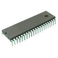
ST72C334N2B6 STMicroelectronics, ST72C334N2B6 Datasheet - Page 109

ST72C334N2B6
Manufacturer Part Number
ST72C334N2B6
Description
Microcontrollers (MCU) Flash 8K SPI/SCI
Manufacturer
STMicroelectronics
Datasheet
1.ST72C334N2T6.pdf
(126 pages)
Specifications of ST72C334N2B6
Data Bus Width
8 bit
Program Memory Type
Flash
Program Memory Size
8 KB
Data Ram Size
384 B
Interface Type
SCI, SPI
Maximum Clock Frequency
8 MHz
Number Of Programmable I/os
44
Number Of Timers
16 bit
Operating Supply Voltage
3.2 V to 5.5 V
Maximum Operating Temperature
+ 85 C
Mounting Style
Through Hole
Package / Case
SDIP-56
Minimum Operating Temperature
- 40 C
On-chip Adc
8 bit
Lead Free Status / Rohs Status
No
Available stocks
Company
Part Number
Manufacturer
Quantity
Price
Company:
Part Number:
ST72C334N2B6
Manufacturer:
ST
Quantity:
365
8.6 SUPPLY, RESET AND CLOCK CHARACTERISTICS
8.6.1 Supply Manager
Recommended operating conditions
with T
8.6.2 Reset Sequence Manager
Recommended operating conditions
with T
8.6.3 Multi-Oscillator, Clock Security System
Recommended operating conditions
with T
Notes:
1) LVD typical data are based on T
2) The V
3) Data based on characterization results, not tested in production.
4) Unless otherwise specified, typical data are based on T
lines and are not tested.
LOW VOLTAG E DETECTOR (LVD)
RESET SEQUENCE MANAGER (RSM)
EXTERNAL CLOCK SOURCE
V
V
V
I
R
t
t
V
V
DD
DELAYmin
PULSE
Symbol
Symbol
Symbol
LVDr
LVDf
LVDhyst
OSC1h
OSC1l
ON
A
A
A
=-40 to +85
=-40...+85
=-40 to +85
LVDhyst
Reset release threshold
(V
Reset generation threshold
(V
V
LVD Supply Current
Reset weak pull-up resistance
Reset delay for external and
watchdog reset sources
External RESET pin Pulse time
OSC1 input pin high level voltage
OSC1 input pin low level voltage
LVD
DD
DD
hysteresis is constant.
rise)
fall)
Hysteresis
o
C and 4.5V<V
o
o
C and voltage are referred to V
C and voltage are referred to V
Parameter
Parameter
Parameter
2)
A
=25 C. They are given only as design guidelines and are not tested.
DD
-V
SS
<5.5V unless otherwise specified.
High Threshold
Med. Threshold (f
Low Threshold (f
High Threshold
Med. Threshold (f
Low Threshold (f
with ~50% Duty Cycle
Square wave signal
A
=25 C and V
SS
SS
V
HALT mode
Condition s
Condition s
Condition s
LVDr
V
V
unless otherwise specified.
unless otherwise specified.
IN
IN
> V
- V
< V
OSC
OSC
LVDf
OSC
OSC
IH
IL
ST72334J/N, ST72314J/N, ST72124J
DD
8MHz)
8MHz)
-V
16MHz)
16MHz)
SS
=5V. They are given only as design guide-
0.7xV
3.85
3.50
3.00
Min
Min
Min
40
20
V
5
SS
DD
Typ
Typ
250*
Typ
4.30
3.90
3.35
4.05
3.65
3.10
100
10
80
30
6
1)
4)
0.3xV
150
Max
Max
Max
4.50
4.05
3.45
4.25
3.80
3.20
160
V
20
DD
3)
DD
1/f
109/125
Unit
Unit
Unit
SFOSC
mV
k
V
V
A
s
s


