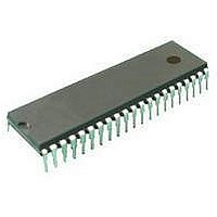
ST72C334N2B6 STMicroelectronics, ST72C334N2B6 Datasheet - Page 18

ST72C334N2B6
Manufacturer Part Number
ST72C334N2B6
Description
Microcontrollers (MCU) Flash 8K SPI/SCI
Manufacturer
STMicroelectronics
Datasheet
1.ST72C334N2T6.pdf
(126 pages)
Specifications of ST72C334N2B6
Data Bus Width
8 bit
Program Memory Type
Flash
Program Memory Size
8 KB
Data Ram Size
384 B
Interface Type
SCI, SPI
Maximum Clock Frequency
8 MHz
Number Of Programmable I/os
44
Number Of Timers
16 bit
Operating Supply Voltage
3.2 V to 5.5 V
Maximum Operating Temperature
+ 85 C
Mounting Style
Through Hole
Package / Case
SDIP-56
Minimum Operating Temperature
- 40 C
On-chip Adc
8 bit
Lead Free Status / Rohs Status
No
Available stocks
Company
Part Number
Manufacturer
Quantity
Price
Company:
Part Number:
ST72C334N2B6
Manufacturer:
ST
Quantity:
365
ST72334J/N, ST72314J/N, ST72124J
DATA EEPROM (Cont’d)
2.6.3 Memory Access
The Data EEPROM memory read/write access
modes are controlled by the LAT bit of the EEP-
ROM Control/Status register (EECSR). The flow-
chart in Figure 8 describes these different memory
access modes.
Read Operation (LAT=0)
The EEPROM can be read as a normal ROM loca-
tion when the LAT bit of the EECSR register is
cleared. In a read cycle, the byte to be accessed is
put on the data bus in less than 1 CPU clock cycle.
This means that reading data from EEPROM
takes the same time as reading data from
EPROM, but this memory cannot be used to exe-
cute machine code.
Write Operation (LAT=1)
To access the write mode, the LAT bit has to be
set by software (the PGM bit remains cleared).
When a write access to the EEPROM area occurs,
the value is latched inside the 16 data latches ac-
cording to its address.
Figure 8. Data EEPROM Programming Flowchart
18/125
IN EEPROM AREA
READ MODE
READ BYTES
INTERRUPT GENERATION
CLEARED BY HARDWARE
PGM=0
LAT=0
IF IE=1
(with the same 12 MSB of the address)
When PGM bit is set by the software, all the previ-
ous bytes written in the data latches (up to 16) are
programmed in the EEPROM cells. The effective
high address (row) is determined by the last EEP-
ROM write sequence. To avoid wrong program-
ming, the user must take care that all the bytes
written between two programming sequences
have the same high address: only the four Least
Significant Bits of the address can change.
At the end of the programming cycle, the PGM and
LAT bits are cleared simultaneously, and an inter-
rupt is generated if the IE bit is set. The Data EEP-
ROM interrupt request is cleared by hardware
when the Data EEPROM interrupt vector is
fetched.
Note: Care should be taken during the program-
ming cycle. Writing to the same memory location
will over-program the memory (logical AND be-
tween the two write access data result) because
the data latches are only cleared at the end of the
programming cycle and by the falling edge of LAT
bit.
It is not possible to read the latched data.
This note is ilustrated by the Figure 9.
START PROGRAMMING CYCLE
WRITE UP TO 16 BYTES
PGM=1 (set by software)
0
IN EEPROM AREA
WRITE MODE
PGM=0
LAT=1
LAT=1
LAT
1


