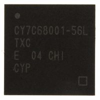
CY7C68001-56LTXC Cypress Semiconductor Corp, CY7C68001-56LTXC Datasheet - Page 17

CY7C68001-56LTXC
Manufacturer Part Number
CY7C68001-56LTXC
Description
IC USB EZ-USB SX2 HS 56VQFN
Manufacturer
Cypress Semiconductor Corp
Series
CY7Cr
Type
USBr
Specifications of CY7C68001-56LTXC
Protocol
USB 2.0
Voltage - Supply
3 V ~ 3.6 V
Mounting Type
Surface Mount
Package / Case
56-VQFN Exposed Pad, 56-HVQFN, 56-SQFN, 56-DHVQFN
Lead Free Status / RoHS Status
Lead free / RoHS Compliant
Number Of Drivers/receivers
-
Lead Free Status / Rohs Status
Lead free / RoHS Compliant
Other names
428-2932
Available stocks
Company
Part Number
Manufacturer
Quantity
Price
Part Number:
CY7C68001-56LTXC
Manufacturer:
CYPRESS/赛普拉斯
Quantity:
20 000
For an OUT set-up transaction, the external master can read each packet received from the USB host during the data phase.
The steps to read a packet are as follows:
To receive more than 64 bytes, the process is repeated. The SX2 internally stores the length of the data phase that was specified
in the wLength field of the set-up packet (bytes 6,7). When the SX2 sees that the specified number of bytes have been received,
it will complete the set-up transfer by automatically completing the handshake phase. If the external master does not wish to
receive the entire transfer, it can stall the transfer.
If the SX2 receives another set-up packet before the current transfer has completed, it will interrupt the external master with
another SETUP interrupt.
If the SX2 receives a set-up packet with no data phase, the external master can accept the packet and complete the handshake
phase by writing zero to the byte count register.
6.0
6.1
Note:
Document #: 38-08013 Rev. *B
1. Wait for an EP0BUF interrupt, indicating that a packet was received from the USB host into the buffer.
2. Initiate a read request for the byte count register, 0x33. This indicates the amount of data received from the host.
3. Initiate a read request for register 0x31.
4. Read one byte.
5. Repeat steps 3 and 4 until the number of bytes specified in the byte count register has been read.
6.
A * denotes programmable polarity.
56-pin SSOP
Pin Assignments
Figure 6-1. CY7C68001 56-pin SSOP Pin Assignment
10
11
12
13
14
15
16
17
18
19
20
21
22
23
24
25
26
27
28
1
2
3
4
5
6
7
8
9
FD13
FD14
FD15
GND
NC
VCC
GND
*SLRD
*SLWR
AVCC
XTALOUT
XTALIN
AGND
VCC
DPLUS
DMINUS
GND
VCC
GND
*IFCLK
RESERVED
SCL
SDA
VCC
FD0
FD1
FD2
FD3
CY7C68001
56-pin SSOP
*FLAGD/CS#
FIFOADR1
FIFOADR0
FIFOADR2
*WAKEUP
*PKTEND
RESET#
*FLAGC
*FLAGB
*FLAGA
READY
*SLOE
FD12
FD11
FD10
GND
GND
GND
INT#
VCC
VCC
VCC
FD9
FD8
FD7
FD6
FD5
FD4
56
55
54
53
52
51
50
49
48
47
46
45
44
43
42
41
40
39
38
37
36
35
34
33
32
31
30
29
[6]
CY7C68001
Page 17 of 50


