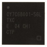
CY7C68001-56LTXC Cypress Semiconductor Corp, CY7C68001-56LTXC Datasheet - Page 15

CY7C68001-56LTXC
Manufacturer Part Number
CY7C68001-56LTXC
Description
IC USB EZ-USB SX2 HS 56VQFN
Manufacturer
Cypress Semiconductor Corp
Series
CY7Cr
Type
USBr
Specifications of CY7C68001-56LTXC
Protocol
USB 2.0
Voltage - Supply
3 V ~ 3.6 V
Mounting Type
Surface Mount
Package / Case
56-VQFN Exposed Pad, 56-HVQFN, 56-SQFN, 56-DHVQFN
Lead Free Status / RoHS Status
Lead free / RoHS Compliant
Number Of Drivers/receivers
-
Lead Free Status / Rohs Status
Lead free / RoHS Compliant
Other names
428-2932
Available stocks
Company
Part Number
Manufacturer
Quantity
Price
Part Number:
CY7C68001-56LTXC
Manufacturer:
CYPRESS/赛普拉斯
Quantity:
20 000
3.7.8.1 Write Request Example
Prior to writing to a register, two conditions must be met: FIFOADR[2:0] must hold [1 0 0], and the Ready line must be HIGH. The
external master should not initiate a command if the READY pin is not in a HIgh state.
Example: to write the byte <10110000> into the IFCONFIG register (0x01), first send a command address byte as follows.
Table 3-7. Command Address Write Byte
Once the byte has been received the SX2 pulls the READY pin low to inform the external master not to send any more information.
When the SX2 is ready to receive the next byte, the SX2 pulls the READY pin high again. Next, the upper nibble of the data byte
is written to the SX2 as follows.
Table 3-8. Command Data Write Byte One
Next, the lower nibble of the data byte is written to the SX2:
Table 3-9. Command Data Write Byte Two
At this point the entire byte <10110000> has been transferred to register 0x01 and the write sequence is complete.
3.7.8.2 Read Request Example
The Read cycle is simpler than the write cycle. The Read cycle consists of a read request from the external master to the SX2.
For example, to read the contents of register 0x01, a command address byte is written to the SX2 as follows.
Table 3-10. Command Address Read Byte
When the data is ready to be read, the SX2 asserts the INT# pin to tell the external master that the data it requested is waiting
on FD[7:0].
4.0
The SX2 has two modes of enumeration. The first mode is automatic through EEPROM boot load, as described in section 3.3.
The second method is a manual load of the descriptor or VID, PID, and DID as described below.
4.1
The SX2 has 500 bytes of descriptor RAM into which the external master may write its descriptor. The descriptor RAM is accessed
through register 0x30. To load a descriptor, the external master does the following:
Notes:
Document #: 38-08013 Rev. *B
4.
5.
• The first bit signifies an address transfer.
• The second bit signifies that this is a write command.
• The next six bits represent the register address (000001 binary = 0x01 hex).
• The first bit signifies that this is a data transfer.
• The next three are don’t care bits.
• The next four bits hold the upper nibble of the transferred byte.
• Initiate a Write Request to register 0x30.
• Write two bytes (four command data transfers) that define the length of the entire descriptor about to be transferred. The LSB
• Write the descriptor, one byte at a time until complete.
is written first, followed by the MSB.
Address/Data#
Address/Data#
Address/Data#
Address/Data#
An important note: Once the SX2 receives a Read request, the SX2 allocates the interrupt line solely for the read request. If one of the six interrupt sources
described in Section 3.4 is asserted, the SX2 will buffer that interrupt until the read request completes.
These and all other data bytes must conform to the command protocol.
1
0
1
Standard Enumeration
0
Enumeration
[4]
Read/Write#
Read/Write#
Don’t Care
Don’t Care
0
X
1
X
Don’t Care
[5]
Don’t Care
A5
A5
0
0
X
X
Don’t Care
Don’t Care
A4
A4
0
0
[5]
X
X
Note: the register address is only written once.
A3
A3
D7
0
0
1
D3
0
A2
A2
D6
0
0
D2
0
0
A1
A1
D5
D1
0
0
0
1
CY7C68001
Page 15 of 50
A0
A0
D0
1
D4
1
0
1


