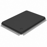
DS21Q42T+ Maxim Integrated Products, DS21Q42T+ Datasheet - Page 50

DS21Q42T+
Manufacturer Part Number
DS21Q42T+
Description
IC FRAMER ENHANCED T1 4X 128TQFP
Manufacturer
Maxim Integrated Products
Datasheet
1.DS21Q42T.pdf
(116 pages)
Specifications of DS21Q42T+
Controller Type
T1 Framer
Interface
Parallel/Serial
Voltage - Supply
2.97 V ~ 3.63 V
Current - Supply
75mA
Operating Temperature
0°C ~ 70°C
Mounting Type
Surface Mount
Package / Case
128-TQFP, 128-VQFP
Lead Free Status / RoHS Status
Lead free / RoHS Compliant
- Current page: 50 of 116
- Download datasheet (950Kb)
RDS0M: RECEIVE DS0 MONITOR REGISTER (Address=1F Hex)
10.
Each framer in the DS21Q42 contains provisions for both processor based (i.e., software based) signaling
bit access and for hardware based access. Both the processor based access and the hardware based access
can be used simultaneously if necessary. The processor based signaling is covered in Section 10.1 and
the hardware based signaling is covered in Section 10.2.
10.1 Processor-Based Signaling
The robbed–bit signaling bits embedded in the T1 stream can be extracted from the receive stream and
inserted into the transmit stream by each framer. There is a set of 12 registers for the receive side (RS1 to
RS12) and 12 registers on the transmit side (TS1 to TS12). The signaling registers are detailed below.
The CCR1.5 bit is used to control the robbed signaling bits as they appear at RSER. If CCR1.5 is set to
zero, then the robbed signaling bits will appear at the RSER pin in their proper position as they are
received. If CCR1.5 is set to a one, then the robbed signaling bit positions will be forced to a one at
RSER. If hardware based signaling is being used, then CCR1.5 must be set to zero.
(MSB)
B1
SYMBOL
SYMBOL
RCM3
RCM2
RCM1
RCM0
SIGNALING OPERATION
B1
B2
B3
B4
B5
B6
B7
B8
B2
POSITION
POSITION
RDS0M.7
RDS0M.6
RDS0M.5
RDS0M.4
RDS0M.3
RDS0M.2
RDS0M.1
RDS0M.0
CCR6.3
CCR6.2
CCR6.1
CCR6.0
B3
NAME AND DESCRIPTION
Receive Channel Monitor Bit 3.
Receive Channel Monitor Bit 2.
Receive Channel Monitor Bit 1.
Receive Channel Monitor Bit 0. LSB of the channel decode.
NAME AND DESCRIPTION
Receive DS0 Channel Bit 1. MSB of the DS0 channel (first
bit to be received).
Receive DS0 Channel Bit 2.
Receive DS0 Channel Bit 3.
Receive DS0 Channel Bit 4.
Receive DS0 Channel Bit 5.
Receive DS0 Channel Bit 6.
Receive DS0 Channel Bit 7.
Receive DS0 Channel Bit 8. LSB of the DS0 channel (last bit
to be received).
B4
50 of 116
B5
B6
B7
(LSB)
B8
Related parts for DS21Q42T+
Image
Part Number
Description
Manufacturer
Datasheet
Request
R

Part Number:
Description:
MAX7528KCWPMaxim Integrated Products [CMOS Dual 8-Bit Buffered Multiplying DACs]
Manufacturer:
Maxim Integrated Products
Datasheet:

Part Number:
Description:
Single +5V, fully integrated, 1.25Gbps laser diode driver.
Manufacturer:
Maxim Integrated Products
Datasheet:

Part Number:
Description:
Single +5V, fully integrated, 155Mbps laser diode driver.
Manufacturer:
Maxim Integrated Products
Datasheet:

Part Number:
Description:
VRD11/VRD10, K8 Rev F 2/3/4-Phase PWM Controllers with Integrated Dual MOSFET Drivers
Manufacturer:
Maxim Integrated Products
Datasheet:

Part Number:
Description:
Highly Integrated Level 2 SMBus Battery Chargers
Manufacturer:
Maxim Integrated Products
Datasheet:

Part Number:
Description:
Current Monitor and Accumulator with Integrated Sense Resistor; ; Temperature Range: -40°C to +85°C
Manufacturer:
Maxim Integrated Products

Part Number:
Description:
TSSOP 14/A�/RS-485 Transceivers with Integrated 100O/120O Termination Resis
Manufacturer:
Maxim Integrated Products

Part Number:
Description:
TSSOP 14/A�/RS-485 Transceivers with Integrated 100O/120O Termination Resis
Manufacturer:
Maxim Integrated Products

Part Number:
Description:
QFN 16/A�/AC-DC and DC-DC Peak-Current-Mode Converters with Integrated Step
Manufacturer:
Maxim Integrated Products

Part Number:
Description:
TDFN/A/65V, 1A, 600KHZ, SYNCHRONOUS STEP-DOWN REGULATOR WITH INTEGRATED SWI
Manufacturer:
Maxim Integrated Products

Part Number:
Description:
Integrated Temperature Controller f
Manufacturer:
Maxim Integrated Products

Part Number:
Description:
SOT23-6/I�/45MHz to 650MHz, Integrated IF VCOs with Differential Output
Manufacturer:
Maxim Integrated Products

Part Number:
Description:
SOT23-6/I�/45MHz to 650MHz, Integrated IF VCOs with Differential Output
Manufacturer:
Maxim Integrated Products

Part Number:
Description:
EVALUATION KIT/2.4GHZ TO 2.5GHZ 802.11G/B RF TRANSCEIVER WITH INTEGRATED PA
Manufacturer:
Maxim Integrated Products

Part Number:
Description:
QFN/E/DUAL PCIE/SATA HIGH SPEED SWITCH WITH INTEGRATED BIAS RESISTOR
Manufacturer:
Maxim Integrated Products
Datasheet:


