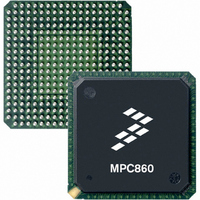
MPC855TCVR50D4 Freescale Semiconductor, MPC855TCVR50D4 Datasheet - Page 43

MPC855TCVR50D4
Manufacturer Part Number
MPC855TCVR50D4
Description
IC MPU POWERQUICC 50MHZ 357PBGA
Manufacturer
Freescale Semiconductor
Datasheets
1.MPC855TVR50D4.pdf
(15 pages)
2.MPC8555ECVTALF.pdf
(88 pages)
3.MPC855TCVR50D4.pdf
(80 pages)
Specifications of MPC855TCVR50D4
Processor Type
MPC8xx PowerQUICC 32-Bit
Speed
50MHz
Voltage
3.3V
Mounting Type
Surface Mount
Package / Case
357-PBGA
Processor Series
MPC8xx
Core
MPC8xx
Data Bus Width
32 bit
Maximum Clock Frequency
50 MHz
Operating Supply Voltage
2.5 V, 3.3 V
Maximum Operating Temperature
+ 95 C
Mounting Style
SMD/SMT
Minimum Operating Temperature
- 40 C
Family Name
MPC8xx
Device Core
PowerQUICC
Device Core Size
32b
Frequency (max)
50MHz
Instruction Set Architecture
RISC
Supply Voltage 1 (typ)
2.5/3.3V
Operating Supply Voltage (max)
3.465/3.6V
Operating Supply Voltage (min)
2/3.135V
Operating Temp Range
-40C to 95C
Operating Temperature Classification
Industrial
Mounting
Surface Mount
Pin Count
357
Package Type
BGA
Lead Free Status / RoHS Status
Lead free / RoHS Compliant
Features
-
Lead Free Status / Rohs Status
Lead free / RoHS Compliant
Available stocks
Company
Part Number
Manufacturer
Quantity
Price
Company:
Part Number:
MPC855TCVR50D4
Manufacturer:
FREESCAL
Quantity:
246
Company:
Part Number:
MPC855TCVR50D4
Manufacturer:
Freescale Semiconductor
Quantity:
10 000
Company:
Part Number:
MPC855TCVR50D4R2
Manufacturer:
Freescale Semiconductor
Quantity:
10 000
10 CPM
This section describes the DC and AC electrical specifications for the CPM of the MPC8555E.
10.1
Table 32
10.2
Table 33
Freescale Semiconductor
Input high voltage
Input low voltage
Output high voltage
Output low voltage
Output high voltage
Output low voltage
Note:
1. This specification applies to the following pins: PA[0–31], PB[4–31], PC[0–31], and PD[4–31].
2. V
FCC inputs—internal clock (NMSI) input setup time
FCC inputs—internal clock (NMSI) hold time
FCC inputs—external clock (NMSI) input setup time
FCC inputs—external clock (NMSI) hold time
SCC/SMC/SPI inputs—internal clock (NMSI) input setup time
SCC/SMC/SPI inputs—internal clock (NMSI) input hold time
SCC/SMC/SPI inputs—external clock (NMSI) input setup time
SCC/SMC/SPI inputs—external clock (NMSI) input hold time
TDM inputs/SI—input setup time
IL
(max) for the IIC interface is 0.8 V rather than the 1.5 V specified in the IIC standard
MPC8555E PowerQUICC™ III Integrated Communications Processor Hardware Specification, Rev. 4.2
provides the DC electrical characteristics for the CPM.
and
CPM DC Electrical Characteristics
CPM AC Timing Specifications
Characteristic
Table 34
It is recommended that the rise/fall time on CPM input pins should not
exceed 5 ns. This should be enforced especially on clock signals. Rise time
refers to signal transitions from 10% to 90% of VCC; fall time refers to
transitions from 90% to 10% of VCC.
provide the CPM input and output AC timing specifications, respectively.
Table 33. CPM Input AC Timing Specifications
Characteristic
Table 32. CPM DC Electrical Characteristics
NOTE: Rise/Fall Time on CPM Input Pins
Symbol
V
V
V
V
V
V
OH
OH
OL
OL
IH
IL
I
I
OH
OH
I
I
OL
OL
Condition
= –8.0 mA
= –2.0 mA
= 3.2 mA
= 8.0 mA
GND
Min
2.0
2.4
2.4
—
—
Symbol
1
t
FEIXKH
t
t
t
t
t
t
t
t
NEIVKH
NEIXKH
FEIVKH
TDIVKH
FIIVKH
FIIXKH
NIIVKH
NIIXKH
3.465
b
Max
2
0.8
0.5
0.4
—
—
Min
2.5
6
0
2
6
0
4
2
4
Unit
3
V
V
V
V
V
V
Notes
Unit
ns
ns
ns
ns
ns
ns
ns
ns
ns
1, 2
1
1
1
1
1
CPM
43


