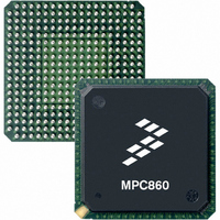
MPC855TCVR50D4 Freescale Semiconductor, MPC855TCVR50D4 Datasheet - Page 23

MPC855TCVR50D4
Manufacturer Part Number
MPC855TCVR50D4
Description
IC MPU POWERQUICC 50MHZ 357PBGA
Manufacturer
Freescale Semiconductor
Datasheets
1.MPC855TVR50D4.pdf
(15 pages)
2.MPC8555ECVTALF.pdf
(88 pages)
3.MPC855TCVR50D4.pdf
(80 pages)
Specifications of MPC855TCVR50D4
Processor Type
MPC8xx PowerQUICC 32-Bit
Speed
50MHz
Voltage
3.3V
Mounting Type
Surface Mount
Package / Case
357-PBGA
Processor Series
MPC8xx
Core
MPC8xx
Data Bus Width
32 bit
Maximum Clock Frequency
50 MHz
Operating Supply Voltage
2.5 V, 3.3 V
Maximum Operating Temperature
+ 95 C
Mounting Style
SMD/SMT
Minimum Operating Temperature
- 40 C
Family Name
MPC8xx
Device Core
PowerQUICC
Device Core Size
32b
Frequency (max)
50MHz
Instruction Set Architecture
RISC
Supply Voltage 1 (typ)
2.5/3.3V
Operating Supply Voltage (max)
3.465/3.6V
Operating Supply Voltage (min)
2/3.135V
Operating Temp Range
-40C to 95C
Operating Temperature Classification
Industrial
Mounting
Surface Mount
Pin Count
357
Package Type
BGA
Lead Free Status / RoHS Status
Lead free / RoHS Compliant
Features
-
Lead Free Status / Rohs Status
Lead free / RoHS Compliant
Available stocks
Company
Part Number
Manufacturer
Quantity
Price
Company:
Part Number:
MPC855TCVR50D4
Manufacturer:
FREESCAL
Quantity:
246
Company:
Part Number:
MPC855TCVR50D4
Manufacturer:
Freescale Semiconductor
Quantity:
10 000
Company:
Part Number:
MPC855TCVR50D4R2
Manufacturer:
Freescale Semiconductor
Quantity:
10 000
Supply voltage 3.3 V
Output high voltage
Output low voltage
Input high voltage
Input low voltage
Input high current
Input low current
Note:
1. The symbol V
Freescale Semiconductor
Supply voltage 2.5 V
Output high voltage (LV
Output low voltage (LV
Input high voltage (LV
Input low voltage (LV
Input high current (V
Input low current (V
Note:
1. Note that the symbol V
Parameter
MPC8555E PowerQUICC™ III Integrated Communications Processor Hardware Specification, Rev. 4.2
IN
, in this case, represents the LV
Parameters
IN
IN
DD
Table 19. GMII, MII, RGMII RTBI, and TBI DC Electrical Characteristics
DD
1
DD
1
DD
= GND)
= Min)
= LV
= Min)
IN
= Min, I
= Min, I
, in this case, represents the LV
Table 18. GMII, MII, and TBI DC Electrical Characteristics
DD
Symbol
)
LV
V
V
V
V
I
I
OL
OH
IH
OL
IL
IH
DD
IL
OH
= 1.0 mA)
= –1.0 mA)
I
OH
I
OL
IN
= –4.0 mA
= 4.0 mA
—
—
symbol referenced in
Symbol
V
V
LV
Conditions
V
V
V
V
IN
IN
I
I
OH
IH
OL
IL
DD
IH
IL
IN
1
1
—
= LV
= GND
symbol referenced in
DD
LV
LV
DD
DD
GND – 0.3
—
—
Table 1
= Min
= Min
2.37
2.00
1.70
–0.3
Min
–15
—
and
Table
Table
GND
–600
3.13
2.40
1.70
–0.3
Ethernet: Three-Speed, MII Management
Min
—
1and
2.
LV
LV
Table
DD
DD
Max
2.63
0.40
0.70
10
—
LV
LV
+ 0.3
+ 0.3
2.
DD
DD
Max
3.47
0.90
0.50
40
—
+ 0.3
+ 0.3
Unit
Unit
μA
μA
μA
μA
V
V
V
V
V
V
V
V
V
V
23


