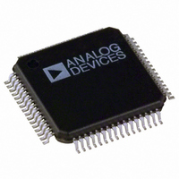
ADE5569ASTZF62 Analog Devices Inc, ADE5569ASTZF62 Datasheet - Page 44

ADE5569ASTZF62
Manufacturer Part Number
ADE5569ASTZF62
Description
IC METER/8052/RTC/LCD DRV 64LQFP
Manufacturer
Analog Devices Inc
Datasheet
1.ADE5569ASTZF62-RL.pdf
(156 pages)
Specifications of ADE5569ASTZF62
Applications
Energy Measurement
Core Processor
8052
Program Memory Type
FLASH (62kB)
Controller Series
ADE55xx
Ram Size
2.25K x 8
Interface
I²C, SPI, UART
Number Of I /o
20
Voltage - Supply
3.135 V ~ 3.465 V
Operating Temperature
-40°C ~ 85°C
Mounting Type
Surface Mount
Package / Case
64-LQFP
Ic Function
Single Phase Energy Measurement IC
Supply Voltage Range
3.13V To 3.46V, 2.4V To 3.7V
Operating Temperature Range
-40°C To +85°C
Digital Ic Case Style
LQFP
No. Of Pins
64
Lead Free Status / RoHS Status
Lead free / RoHS Compliant
Lead Free Status / RoHS Status
Lead free / RoHS Compliant, Lead free / RoHS Compliant
Available stocks
Company
Part Number
Manufacturer
Quantity
Price
Company:
Part Number:
ADE5569ASTZF62
Manufacturer:
Analog Devices Inc
Quantity:
10 000
Company:
Part Number:
ADE5569ASTZF62-RL
Manufacturer:
Analog Devices Inc
Quantity:
10 000
ADE5166/ADE5169/ADE5566/ADE5569
Table 37. Accumulation Mode Register (ACCMODE, Address 0x0F)
Bit
7
6
5
4
3
2
1
0
1
2
Table 38. Gain Register (GAIN, Address 0x1B)
Bit
[7:5]
4
3
[2:0]
Table 39. Mode 3 Register (MODE3, Address 0x2B)
Bit
[7:2]
1
0
This function is not available in the ADE5566 and ADE5569.
This function is not available in the ADE5166 and ADE5566.
Mnemonic
ICHANNEL
FAULTSIGN
VARSIGN
APSIGN
ABSVARM
SAVARM
POAM
ABSAM
Mnemonic
PGA2
Reserved
CFSIGN_OPT
PGA1
Mnemonic
Reserved
ZX1
ZX2
2
2
2
1
1
Default
0
0
0
0
0
0
0
0
Default
000
0
0
000
Default
0
0
0
This bit indicates the current channel used to measure energy in antitampering mode.
0 = Channel A (I
1 = Channel B (I
Configuration bit to select the event that triggers a fault interrupt.
0 = FAULTSIGN interrupt occurs when the part enters fault mode.
Description
1 = FAULTSIGN interrupt occurs when the part enters normal mode.
Configuration bit to select the event that triggers a reactive power sign interrupt.
If cleared to 0, a VARSIGN interrupt occurs when reactive power changes from positive to negative.
If set to 1, a VARSIGN interrupt occurs when reactive power changes from negative to positive.
Configuration bit to select the event that triggers an active power sign interrupt.
If cleared to 0, an APSIGN interrupt occurs when active power changes from positive to negative.
If set to 1, an APSIGN interrupt occurs when active power changes from negative to positive.
Logic 1 enables absolute value accumulation of reactive power in energy register and pulse output.
Logic 1 enables reactive power accumulation depending on the sign of the active power.
If active power is positive, var is accumulated as it is.
If active power is negative, the sign of the var is reversed for the accumulation.
This accumulation mode affects both the var registers (VARHR, RVARHR, LVARHR) and the pulse
output when connected to the reactive measurement.
Logic 1 enables positive-only accumulation of active power in energy register and pulse output.
Logic 1 enables absolute value accumulation of active power in energy register and pulse output.
Description
These bits define the voltage channel input gain.
PGA2
000
001
010
011
100
Reserved.
This bit defines where the CF change of sign detection (APSIGN or VARSIGN) is implemented.
CFSIGN_OPT
0
1
These bits define the current channel input gain.
PGA1
000
001
010
011
100
Description
Reserved.
Setting this bit enables the zero-crossing output signal on P1.2.
Setting this bit enables the zero-crossing output signal on P0.5.
PB
PA
).
).
Rev. C | Page 44 of 156
Result
Gain = 1
Gain = 2
Gain = 4
Gain = 8
Gain = 16
Result
Filtered power signal
On a per CF pulse basis
Result
Gain = 1
Gain = 2
Gain = 4
Gain = 8
Gain = 16
2


