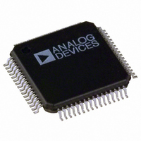
ADE5569ASTZF62 Analog Devices Inc, ADE5569ASTZF62 Datasheet - Page 147

ADE5569ASTZF62
Manufacturer Part Number
ADE5569ASTZF62
Description
IC METER/8052/RTC/LCD DRV 64LQFP
Manufacturer
Analog Devices Inc
Datasheet
1.ADE5569ASTZF62-RL.pdf
(156 pages)
Specifications of ADE5569ASTZF62
Applications
Energy Measurement
Core Processor
8052
Program Memory Type
FLASH (62kB)
Controller Series
ADE55xx
Ram Size
2.25K x 8
Interface
I²C, SPI, UART
Number Of I /o
20
Voltage - Supply
3.135 V ~ 3.465 V
Operating Temperature
-40°C ~ 85°C
Mounting Type
Surface Mount
Package / Case
64-LQFP
Ic Function
Single Phase Energy Measurement IC
Supply Voltage Range
3.13V To 3.46V, 2.4V To 3.7V
Operating Temperature Range
-40°C To +85°C
Digital Ic Case Style
LQFP
No. Of Pins
64
Lead Free Status / RoHS Status
Lead free / RoHS Compliant
Lead Free Status / RoHS Status
Lead free / RoHS Compliant, Lead free / RoHS Compliant
Available stocks
Company
Part Number
Manufacturer
Quantity
Price
Company:
Part Number:
ADE5569ASTZF62
Manufacturer:
Analog Devices Inc
Quantity:
10 000
Company:
Part Number:
ADE5569ASTZF62-RL
Manufacturer:
Analog Devices Inc
Quantity:
10 000
I/O PORTS
PARALLEL I/O
The ADE5166/ADE5169/ADE5566/ADE5569 use three input/
output ports to exchange data with external devices. In addition
to performing general-purpose I/O, some ports are capable of
driving an LCD or performing alternate functions for the periph-
erals available on chip. In general, when a peripheral is enabled, the
pins associated with it cannot be used as general-purpose I/Os. The
I/O port can be configured through the SFRs listed in Table 160.
Table 160. I/O Port SFRs
SFR
P0
P1
P2
EPCFG
PINMAP0
PINMAP1
PINMAP2
The three bidirectional I/O ports have internal pull-ups that can
be enabled or disabled individually for each pin. The internal
pull-ups are enabled by default. Disabling an internal pull-up
causes a pin to become open drain. Weak internal pull-ups are
configured through the PINMAPx SFRs.
Figure 117 shows a typical bit latch and I/O buffer for an I/O pin.
The bit latch (one bit in the SFR of each port) is represented as a
Type D flip-flop, which clocks in a value from the internal bus
in response to a write-to-latch signal from the CPU. The Q out-
put of the flip-flop is placed on the internal bus in response to a
read latch signal from the CPU. The level of the port pin itself is
placed on the internal bus in response to a read pin signal from
the CPU. Some instructions that read a port activate the read
latch signal, and others activate the read pin signal. See the
Read-Modify-Write Instructions section for details.
INTERNAL
TO LATCH
LATCH
WRITE
READ
READ
BUS
PIN
Address
0x80
0x90
0xA0
0x9F
0xB2
0xB3
0xB4
Figure 117. Port 0 Bit Latch and I/O Buffer
LATCH
D
CL
Q
Q
ALTERNATE
ALTERNATE
FUNCTION
FUNCTION
Bit Addressable
Yes
Yes
Yes
No
No
No
No
OUTPUT
INPUT
DV
DD
CLOSED: PINMAPx.x = 0
OPEN: PINMAPx.x = 1
INTERNAL
PULL-UP
Description
Port 0
Port 1
Port 2
Extended port
configuration
Port 0 weak
pull-up enable
Port 1 weak
pull-up enable
Port 2 weak
pull-up enable
Px.x
PIN
Rev. C | Page 147 of 156
Weak Internal Pull-Ups Enabled
A pin with weak internal pull-up enabled is used as an input by
writing a 1 to the pin. The pin is pulled high by the internal pull-
up, and the pin is read using the circuitry shown in Figure 117.
If the pin is driven low externally, it sources current because of
the internal pull-up.
A pin with internal pull-up enabled is used as an output by writing
a 1 or a 0 to the pin to control the level of the output. If a 0 is
written to the pin, it drives a logic low output voltage (V
is capable of sinking 1.6 mA.
Open Drain (Weak Internal Pull-Ups Disabled)
When the weak internal pull-up on a pin is disabled, the pin
becomes open drain. Use this open-drain pin as a high impedance
input by writing a 1 to the pin. The pin is read using the circuitry
shown in Figure 117. The open-drain option is preferable for
inputs because it draws less current than the internal pull-ups
that were enabled.
38 kHz Modulation
Each ADE5166/ADE5169/ADE5566/ADE5569 provides a 38 kHz
modulation signal. The 38 kHz modulation is accomplished by
internally XOR’ing the level written to the I/O pin with a 38 kHz
square wave. Then, when a 0 is written to the I/O pin, it is
modulated as shown in Figure 118.
Uses for this 38 kHz modulation include IR modulation of
a UART transmit signal or a low power signal to drive an LED.
The modulation can be enabled or disabled with the MOD38EN
bit in the configuration SFR (CFG, Address 0xAF[4]). The 38 kHz
modulation is available on eight pins, which are selected by the
MOD38 bits in the extended port configuration SFR (EPCFG,
Address 0x9F[7:0]).
38kHz MODULATION
ADE5166/ADE5169/ADE5566/ADE5569
38kHz MODULATED
LEVEL WRITTEN
OUTPUT PIN
TO MOD38
SIGNAL
Figure 118. 38 kHz Modulation
OL
) and


