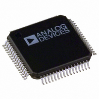
ADE5569ASTZF62 Analog Devices Inc, ADE5569ASTZF62 Datasheet - Page 145

ADE5569ASTZF62
Manufacturer Part Number
ADE5569ASTZF62
Description
IC METER/8052/RTC/LCD DRV 64LQFP
Manufacturer
Analog Devices Inc
Datasheet
1.ADE5569ASTZF62-RL.pdf
(156 pages)
Specifications of ADE5569ASTZF62
Applications
Energy Measurement
Core Processor
8052
Program Memory Type
FLASH (62kB)
Controller Series
ADE55xx
Ram Size
2.25K x 8
Interface
I²C, SPI, UART
Number Of I /o
20
Voltage - Supply
3.135 V ~ 3.465 V
Operating Temperature
-40°C ~ 85°C
Mounting Type
Surface Mount
Package / Case
64-LQFP
Ic Function
Single Phase Energy Measurement IC
Supply Voltage Range
3.13V To 3.46V, 2.4V To 3.7V
Operating Temperature Range
-40°C To +85°C
Digital Ic Case Style
LQFP
No. Of Pins
64
Lead Free Status / RoHS Status
Lead free / RoHS Compliant
Lead Free Status / RoHS Status
Lead free / RoHS Compliant, Lead free / RoHS Compliant
Available stocks
Company
Part Number
Manufacturer
Quantity
Price
Company:
Part Number:
ADE5569ASTZF62
Manufacturer:
Analog Devices Inc
Quantity:
10 000
Company:
Part Number:
ADE5569ASTZF62-RL
Manufacturer:
Analog Devices Inc
Quantity:
10 000
Table 159. I
Bit
7
6
5
4
[3:2]
1
0
READ AND WRITE OPERATIONS
Figure 114 and Figure 115 depict I
respectively. Note that the LSB of the I2CADR SFR (Address 0xE9)
is used to select whether a read or write operation is performed
on the slave device. During the read operation, the master acknowl-
edgements are generated automatically by the I
master-generated no acknowledge (NACK) before the end of
a read operation is also automatically generated after the I2CRCT
bits in the I2CMOD SFR (Address 0xE8[4:0]) have been read from
the slave. If the I2CADR register is updated during a transmission,
the master generates a start condition instead of a stop at the end
of the read or write operation and then continues with the next
communication.
SDATA
SCLK
START BY
MASTER
Mnemonic
I2CBUSY
I2CNOACK
I2CRxIRQ
I2CTxIRQ
I2CFIFOSTAT
I2CACC_ERR
I2CTxWR_ERR
A6
2
1
C Interrupt Status SFR (SPI2CSTAT, Address 0xEA)
SERIAL BUS ADDRESS BYTE
A5
SDATA
SCLK
A4
START BY
MASTER
FRAME 1
A3
A2
Default
0
0
0
0
00
0
0
A6
1
A1
2
C read and write operations,
A5
SERIAL BUS ADDRESS BYTE
A0
This bit is set to Logic 1 when the I
I
does not send an acknowledgement. The I
Write a 0 to this bit to clear it.
I
Write a 0 to this bit to clear it.
I
Write a 0 to this bit to clear it.
Status bits for 3- or 4-byte deep I
used in I
I2CFIFOSTAT
00
01
10
11
Set when trying to write and read at the same time. Write a 0 to this bit to clear it.
Set when a write is attempted when the I
A4
Description
R/W
2
2
2
C no acknowledgement transmit interrupt. This bit is set to Logic 1 when the slave device
C receive interrupt. This bit is set to Logic 1 when the receive FIFO is not empty.
C transmit interrupt. This bit is set to Logic 1 when the transmit FIFO is empty.
ACK BY
SLAVE
FRAME 1
A3
2
C peripheral. The
9
2
A2
D7
C communication (receive or transmit) because only one FIFO is active at a time.
1
A1
D6
DATA BYTE 1 FROM MASTER
Figure 115. I
Figure 114. I
D5
A0
Rev. C | Page 145 of 156
R/W
D4
ACK BY
SLAVE
FRAME 2
Result
FIFO full
FIFO empty
Reserved
FIFO half full
D3
9
2
2
C Write Operation
C Read Operation
D2
D7
1
2
C FIFO. The FIFO monitored in these two bits is the one currently
D1
Reading the SPI/I
Address 0x9B)
Reading the SPI2CRx SFR should be done with a 2-cycle
instruction, such as
Mov a, spi2crx or Mov R0, spi2crx .
A 3-cycle instruction, such as
Mov 3dh, spi2crx
does not transfer the right data into RAM Address 0x3D.
2
D6
C interface is used. When set, the Tx FIFO is emptied.
DATA BYTE 1 FROM MASTER
ADE5166/ADE5169/ADE5566/ADE5569
D0
D5
ACK BY
MASTER
2
C transmit FIFO is full. Write a 0 to this bit to clear it.
2
9
C communication is stopped after this event.
D4
FRAME 2
D3
D2
D7
1
2
C Receive Buffer SFR (SPI2CRx,
D6
D1
DATA BYTE N FROM SLAVE
D5
D0
ACK BY
SLAVE
D4
9
FRAME N + 1
D3
STOP BY
MASTER
D2
D1
D0
NACK BY
MASTER
9
STOP BY
MASTER


