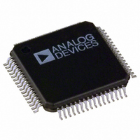
ADE5569ASTZF62 Analog Devices Inc, ADE5569ASTZF62 Datasheet - Page 24

ADE5569ASTZF62
Manufacturer Part Number
ADE5569ASTZF62
Description
IC METER/8052/RTC/LCD DRV 64LQFP
Manufacturer
Analog Devices Inc
Datasheet
1.ADE5569ASTZF62-RL.pdf
(156 pages)
Specifications of ADE5569ASTZF62
Applications
Energy Measurement
Core Processor
8052
Program Memory Type
FLASH (62kB)
Controller Series
ADE55xx
Ram Size
2.25K x 8
Interface
I²C, SPI, UART
Number Of I /o
20
Voltage - Supply
3.135 V ~ 3.465 V
Operating Temperature
-40°C ~ 85°C
Mounting Type
Surface Mount
Package / Case
64-LQFP
Ic Function
Single Phase Energy Measurement IC
Supply Voltage Range
3.13V To 3.46V, 2.4V To 3.7V
Operating Temperature Range
-40°C To +85°C
Digital Ic Case Style
LQFP
No. Of Pins
64
Lead Free Status / RoHS Status
Lead free / RoHS Compliant
Lead Free Status / RoHS Status
Lead free / RoHS Compliant, Lead free / RoHS Compliant
Available stocks
Company
Part Number
Manufacturer
Quantity
Price
Company:
Part Number:
ADE5569ASTZF62
Manufacturer:
Analog Devices Inc
Quantity:
10 000
Company:
Part Number:
ADE5569ASTZF62-RL
Manufacturer:
Analog Devices Inc
Quantity:
10 000
ADE5166/ADE5169/ADE5566/ADE5569
TERMINOLOGY
Measurement Error
The error associated with the energy measurement made by the
ADE5166/ADE5169/ADE5566/ADE5569 is defined by the fol-
lowing formula:
Phase Error Between Channels
The digital integrator and the high-pass filter (HPF) in the current
channel have a nonideal phase response. To offset this phase
response and equalize the phase response between channels,
two phase correction networks are placed in the current channel:
one for the digital integrator and the other for the HPF. The phase
correction networks correct the phase response of the corre-
sponding component and ensure a phase match between the
current channel and the voltage channel to within ±0.1° over a
range of 45 Hz to 65 Hz with the digital integrator off. With the
digital integrator on, the phase is corrected to within ±0.4° over
a range of 45 Hz to 65 Hz.
Power Supply Rejection (PSR)
PSR quantifies the ADE5166/ADE5169/ADE5566/ADE5569
measurement error as a percentage of reading when the power
supplies are varied. For the ac PSR measurement, a reading at
nominal supplies (3.3 V) is taken. A second reading is obtained
Measurement Error =
⎛
⎜
⎜
⎝
Energy
Register
True
Energy
−
True
Energy
⎞
⎟
⎟
⎠
×
100
%
Rev. C | Page 24 of 156
with the same input signal levels when an ac signal (100 mV rms/
120 Hz) is introduced onto the supplies. Any error introduced
by this ac signal is expressed as a percentage of the reading (see
the Measurement Error definition).
For the dc PSR measurement, a reading at nominal supplies
(3.3 V) is taken. A second reading is obtained with the same
input signal levels when the supplies are varied ±5%. Any error
introduced is expressed as a percentage of the reading.
ADC Offset Error
ADC offset error is the dc offset associated with the analog
inputs to the ADCs. It means that, with the analog inputs
connected to AGND, the ADCs still see a dc analog input
signal. The magnitude of the offset depends on the gain and
input range selection. However, when HPF1 is switched on,
the offset is removed from the current channel, and the power
calculation is not affected by this offset. The offsets can be
removed by performing an offset calibration (see the Analog
Inputs section).
Gain Error
Gain error is the difference between the measured ADC output
code (minus the offset) and the ideal output code (see the Current
Channel ADC section and the Voltage Channel ADC section).
It is measured for each of the gain settings on the current channel
(1, 2, 4, 8, and 16). The difference is expressed as a percentage
of the ideal code.


