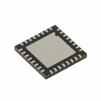
CY8CTMG200-32LQXI Cypress Semiconductor Corp, CY8CTMG200-32LQXI Datasheet - Page 44

CY8CTMG200-32LQXI
Manufacturer Part Number
CY8CTMG200-32LQXI
Description
IC MCU 32K FLASH 32UQFN
Manufacturer
Cypress Semiconductor Corp
Series
TrueTouch™r
Datasheet
1.CY8CTST200-16LGXI.pdf
(308 pages)
Specifications of CY8CTMG200-32LQXI
Program Memory Type
FLASH (32 kB)
Package / Case
32-UQFN Exposed Pad, 32-HUQFN, 32-SQFN
Applications
Touchscreen Controller
Core Processor
M8C
Controller Series
CY8CT
Ram Size
2K x 8
Interface
I²C, SPI, UART/USART, USB
Number Of I /o
28
Voltage - Supply
1.8 V
Operating Temperature
-40°C ~ 85°C
Mounting Type
Surface Mount
Processor Series
CY8CTxx2xx
Core
M8C
Data Bus Width
8 bit
Data Ram Size
2 KB
Interface Type
I2C, SPI
Maximum Clock Frequency
24 MHz
Number Of Timers
3
Operating Supply Voltage
1.71 V to 5.5 V
Mounting Style
SMD/SMT
Program Memory Size
32 KB
Lead Free Status / RoHS Status
Lead free / RoHS Compliant
For Use With
770-1000 - ISP 4PORT FOR CYPRESS PSOC MCU
Lead Free Status / Rohs Status
Lead free / RoHS Compliant
Other names
428-2954
Available stocks
Company
Part Number
Manufacturer
Quantity
Price
Company:
Part Number:
CY8CTMG200-32LQXI
Manufacturer:
CYPRESS
Quantity:
921
Company:
Part Number:
CY8CTMG200-32LQXIT
Manufacturer:
AD
Quantity:
15 186
- Current page: 44 of 308
- Download datasheet (3Mb)
4.2.6
The MVI Write Page Pointer Register (MVW_PP) sets the
effective SRAM page for MVI write memory accesses in a
multi-SRAM page PSoC device.
Bits 2 to 0: Page Bits[2:0]. These bits are only used by the
MVI [expr], A instruction, not to be confused with the
MVI A, [expr] instruction covered by the MVR_PP regis-
ter. This instruction is considered a write because data is
transferred from the microprocessor's A register (CPU_A) to
SRAM.
When an MVI
device with more than one page of SRAM, the SRAM
4.2.7
■
RAM Paging
44
0,D5h
Address
CPU_F Register on page
MVW_PP
MVW_PP Register
Related Registers
Name
[expr],
Bit 7
A instruction is executed in a
32.
Bit 6
PSoC CY8CTMG20x and CY8CTST200 TRM, Document No. 001-53603 Rev. *C
Bit 5
Bit 4
address that is written by the instruction is determined by the
value of the least significant bits in this register. However,
the pointer for the MVI [expr], A instruction is always
located in the current SRAM page. See the PSoC Designer
Assembly Language User Guide for more information on the
MVI [expr], A instruction.
The function of this register and the MVI instructions are
independent of the SRAM Paging bits in the CPU_F register.
For additional information, refer to the
page
238.
Bit 3
Bit 2
Page Bits[2:0]
Bit 1
MVW_PP register on
Bit 0
Access
RW : 0
[+] Feedback
Related parts for CY8CTMG200-32LQXI
Image
Part Number
Description
Manufacturer
Datasheet
Request
R
Part Number:
Description:
CY8CTMG200-32LQXIT
Manufacturer:
Cypress Semiconductor Corp
Datasheet:

Part Number:
Description:
IC MCU 32K FLASH 16-COL
Manufacturer:
Cypress Semiconductor Corp
Datasheet:

Part Number:
Description:
IC MCU 32K FLASH 24UQFN
Manufacturer:
Cypress Semiconductor Corp
Datasheet:

Part Number:
Description:
IC MCU 32K FLASH 48-QFN
Manufacturer:
Cypress Semiconductor Corp
Datasheet:
Part Number:
Description:
IC MCU 32K FLASH 16-COL
Manufacturer:
Cypress Semiconductor Corp
Datasheet:
Part Number:
Description:
IC MCU 32K FLASH 24UQFN
Manufacturer:
Cypress Semiconductor Corp
Datasheet:
Part Number:
Description:
IC MCU 32K FLASH 48-QFN
Manufacturer:
Cypress Semiconductor Corp
Datasheet:
Part Number:
Description:
Manufacturer:
Cypress Semiconductor Corp
Datasheet:
Part Number:
Description:
Manufacturer:
Cypress Semiconductor Corp
Datasheet:


