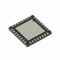
CY8CTMG200-32LQXI Cypress Semiconductor Corp, CY8CTMG200-32LQXI Datasheet - Page 164

CY8CTMG200-32LQXI
Manufacturer Part Number
CY8CTMG200-32LQXI
Description
IC MCU 32K FLASH 32UQFN
Manufacturer
Cypress Semiconductor Corp
Series
TrueTouch™r
Datasheet
1.CY8CTST200-16LGXI.pdf
(308 pages)
Specifications of CY8CTMG200-32LQXI
Program Memory Type
FLASH (32 kB)
Package / Case
32-UQFN Exposed Pad, 32-HUQFN, 32-SQFN
Applications
Touchscreen Controller
Core Processor
M8C
Controller Series
CY8CT
Ram Size
2K x 8
Interface
I²C, SPI, UART/USART, USB
Number Of I /o
28
Voltage - Supply
1.8 V
Operating Temperature
-40°C ~ 85°C
Mounting Type
Surface Mount
Processor Series
CY8CTxx2xx
Core
M8C
Data Bus Width
8 bit
Data Ram Size
2 KB
Interface Type
I2C, SPI
Maximum Clock Frequency
24 MHz
Number Of Timers
3
Operating Supply Voltage
1.71 V to 5.5 V
Mounting Style
SMD/SMT
Program Memory Size
32 KB
Lead Free Status / RoHS Status
Lead free / RoHS Compliant
For Use With
770-1000 - ISP 4PORT FOR CYPRESS PSOC MCU
Lead Free Status / Rohs Status
Lead free / RoHS Compliant
Other names
428-2954
Available stocks
Company
Part Number
Manufacturer
Quantity
Price
Company:
Part Number:
CY8CTMG200-32LQXI
Manufacturer:
CYPRESS
Quantity:
921
Company:
Part Number:
CY8CTMG200-32LQXIT
Manufacturer:
AD
Quantity:
15 186
- Current page: 164 of 308
- Download datasheet (3Mb)
19.2.3
The
(PT2_CFG) configures the PSoC’s programmable timer.
Bit 2: CLKSEL. This bit determines if the timer runs on the
32 kHz clock or CPU clock. If the bit is set to 1'b1, the timer
runs on the CPU clock, otherwise, the timer runs on the 32
kHz clock.
Bit 1: One Shot. This bit determines if the timer runs in
one-shot mode or continuous mode. In one-shot mode the
timer completes one full count cycle and terminates. Upon
termination, the START bit in this register is cleared. In con-
19.2.4
The Programmable Timer Data Register 0 (PT0_DATA0,
PT1_DATA0, PT2_DATA0) holds the lower 8 bits of the pro-
grammable timer’s count value.
Bits 7 to 0: DATA[7:0]. This is the lower byte of a 16-bit
timer. The upper byte is in the corresponding PTxDATA1
register.
19.2.5
The Programmable Timer Data Register 1 (PT0_DATA1,
PT1_DATA1, PT2_DATA1) holds the 8 bits of the program-
mable timer’s count value for the device
Bits 7 to 0: DATA[7:0]. This is the upper byte of a 16-bit
timer. The lower byte is in the corresponding PTx_DATA0
register.
Programmable Timer
164
0,B6h
0,B2h
0,B5h
0,B8h
0,B1h
0,B4h
0,B7h
Address
Address
Address
Programmable
PT2_CFG
PT0_DATA0
PT1_DATA0
PT2_DATA0
PT0_DATA1
PT1_DATA1
PT2_DATA1
PT2_CFG Register
PTx_DATA0 Register
PTx_DATA1 Register
Name
Name
Name
Timer
Bit 7
Bit 7
Bit 7
Configuration
Bit 6
Bit 6
Bit 6
PSoC CY8CTMG20x and CY8CTST200 TRM, Document No. 001-53603 Rev. *C
Bit 5
Bit 5
Bit 5
Register
Bit 4
Bit 4
Bit 4
tinuous mode, the timer reloads the count value each time
upon completion of its count cycle and repeats.
Bit 0: START. This bit starts the timer counting from a full
count. The full count is determined by the value loaded into
the data registers. This bit is cleared when the timer is run-
ning in one-shot mode upon completion of a full count cycle.
For additional information, refer to the
page
For additional information, refer to the
on page
PT2_DATA0 register on page
For additional information, refer to the
on page
PT2_DATA1 register on page
DATA[7:0]
DATA[7:0]
DATA[7:0]
DATA[7:0]
DATA[7:0]
DATA[7:0]
225.
Bit 3
Bit 3
Bit 3
222,
223,
PT1_DATA1 register on page
PT1_DATA0 register on page 223
CLKSEL
Bit 2
Bit 2
Bit 2
One Shot
223.
222.
Bit 1
Bit 1
Bit 1
PT2_CFG register on
PT0_DATA0 register
PT0_DATA1 register
START
Bit 0
Bit 0
Bit 0
222, and
RW : 00
RW : 00
RW : 00
Access
RW : 00
RW : 00
RW : 00
Access
Access
RW : 0
and
[+] Feedback
Related parts for CY8CTMG200-32LQXI
Image
Part Number
Description
Manufacturer
Datasheet
Request
R
Part Number:
Description:
CY8CTMG200-32LQXIT
Manufacturer:
Cypress Semiconductor Corp
Datasheet:

Part Number:
Description:
IC MCU 32K FLASH 16-COL
Manufacturer:
Cypress Semiconductor Corp
Datasheet:

Part Number:
Description:
IC MCU 32K FLASH 24UQFN
Manufacturer:
Cypress Semiconductor Corp
Datasheet:

Part Number:
Description:
IC MCU 32K FLASH 48-QFN
Manufacturer:
Cypress Semiconductor Corp
Datasheet:
Part Number:
Description:
IC MCU 32K FLASH 16-COL
Manufacturer:
Cypress Semiconductor Corp
Datasheet:
Part Number:
Description:
IC MCU 32K FLASH 24UQFN
Manufacturer:
Cypress Semiconductor Corp
Datasheet:
Part Number:
Description:
IC MCU 32K FLASH 48-QFN
Manufacturer:
Cypress Semiconductor Corp
Datasheet:
Part Number:
Description:
Manufacturer:
Cypress Semiconductor Corp
Datasheet:
Part Number:
Description:
Manufacturer:
Cypress Semiconductor Corp
Datasheet:


