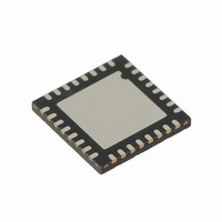
CY8CTMG200-32LQXI Cypress Semiconductor Corp, CY8CTMG200-32LQXI Datasheet - Page 157

CY8CTMG200-32LQXI
Manufacturer Part Number
CY8CTMG200-32LQXI
Description
IC MCU 32K FLASH 32UQFN
Manufacturer
Cypress Semiconductor Corp
Series
TrueTouch™r
Datasheet
1.CY8CTST200-16LGXI.pdf
(308 pages)
Specifications of CY8CTMG200-32LQXI
Program Memory Type
FLASH (32 kB)
Package / Case
32-UQFN Exposed Pad, 32-HUQFN, 32-SQFN
Applications
Touchscreen Controller
Core Processor
M8C
Controller Series
CY8CT
Ram Size
2K x 8
Interface
I²C, SPI, UART/USART, USB
Number Of I /o
28
Voltage - Supply
1.8 V
Operating Temperature
-40°C ~ 85°C
Mounting Type
Surface Mount
Processor Series
CY8CTxx2xx
Core
M8C
Data Bus Width
8 bit
Data Ram Size
2 KB
Interface Type
I2C, SPI
Maximum Clock Frequency
24 MHz
Number Of Timers
3
Operating Supply Voltage
1.71 V to 5.5 V
Mounting Style
SMD/SMT
Program Memory Size
32 KB
Lead Free Status / RoHS Status
Lead free / RoHS Compliant
For Use With
770-1000 - ISP 4PORT FOR CYPRESS PSOC MCU
Lead Free Status / Rohs Status
Lead free / RoHS Compliant
Other names
428-2954
Available stocks
Company
Part Number
Manufacturer
Quantity
Price
Company:
Part Number:
CY8CTMG200-32LQXI
Manufacturer:
CYPRESS
Quantity:
921
Company:
Part Number:
CY8CTMG200-32LQXIT
Manufacturer:
AD
Quantity:
15 186
- Current page: 157 of 308
- Download datasheet (3Mb)
18.3.3
Enable/Disable Operation. As soon as the block is config-
ured for SPI Slave and before enabling, the MISO output is
set to idle at logic 1. The Enable bit must be set and the SS_
asserted (either driven externally or forced by firmware pro-
gramming) for the block to output data. When enabled, the
primary output is the MSb or LSb of the Shift register,
depending on the LSb First configuration in bit 7 of the Con-
trol register. The auxiliary output of the SPIS is always
forced into tristate.
Since the SPIS has no internal clock, it must be enabled
with setup time to any external master supplying the clock.
Setup time is also required for a TX Buffer register write
before the first edge of the clock or the first falling edge of
SS_, depending on the mode. This setup time must be
assured through the protocol and an understanding of the
timing between the master and slave in a system.
PSoC CY8CTMG20x and CY8CTST200 TRM, Document No. 001-53603 Rev. *C
At the falling edge of SS_, MISO
SPIS Timing
transitions from an IDLE (high)
to output the first bit of data.
TX REG EMPTY
SCLK (MODE 0)
SCLK (MODE 1)
SCLK (Internal)
RX REG FULL
User writes first byte to the
TX Buffer register in
advance of transfer.
MISO
SS_
Figure 18-9. Typical SPIS Timing in Modes 0 and 1
First input
latched.
D7
bit is
User writes the next byte
to the TX Buffer register.
Shift.
First
D6
D5
Last bit of received data is valid
on this edge and is latched into
When the block is disabled, the MISO output reverts to its
idle 1 state. All internal state is reset (including CR0 status)
to its configuration-specific reset state, except for DR0,
DR1, and DR2, which are unaffected.
Normal Operation. Typical timing for an SPIS transfer is
shown in
rily being used as a receiver, the RX Reg Full (polling only)
or SPI Complete (polling or interrupt) status may be used to
determine when a byte has been received. In this way, the
SPIS operates identically with the SPIM. However, there are
two main areas in which the SPIS operates differently: 1)
SPIS behavior related to the SS_ signal, and 2) TX data
queuing (loading the TX Buffer register).
the RX Buffer register.
D2
Figure 18-9
D1
and
D0
Figure
D7
18-10. If the SPIS is prima-
D7
D6
157
SPI
[+] Feedback
Related parts for CY8CTMG200-32LQXI
Image
Part Number
Description
Manufacturer
Datasheet
Request
R
Part Number:
Description:
CY8CTMG200-32LQXIT
Manufacturer:
Cypress Semiconductor Corp
Datasheet:

Part Number:
Description:
IC MCU 32K FLASH 16-COL
Manufacturer:
Cypress Semiconductor Corp
Datasheet:

Part Number:
Description:
IC MCU 32K FLASH 24UQFN
Manufacturer:
Cypress Semiconductor Corp
Datasheet:

Part Number:
Description:
IC MCU 32K FLASH 48-QFN
Manufacturer:
Cypress Semiconductor Corp
Datasheet:
Part Number:
Description:
IC MCU 32K FLASH 16-COL
Manufacturer:
Cypress Semiconductor Corp
Datasheet:
Part Number:
Description:
IC MCU 32K FLASH 24UQFN
Manufacturer:
Cypress Semiconductor Corp
Datasheet:
Part Number:
Description:
IC MCU 32K FLASH 48-QFN
Manufacturer:
Cypress Semiconductor Corp
Datasheet:
Part Number:
Description:
Manufacturer:
Cypress Semiconductor Corp
Datasheet:
Part Number:
Description:
Manufacturer:
Cypress Semiconductor Corp
Datasheet:


